How CMP Creates an Ultra-Flat Semiconductor Surface
💻 iAtlas Semiconductor #9 | 📘 Manufacturing → CMP
Introduction
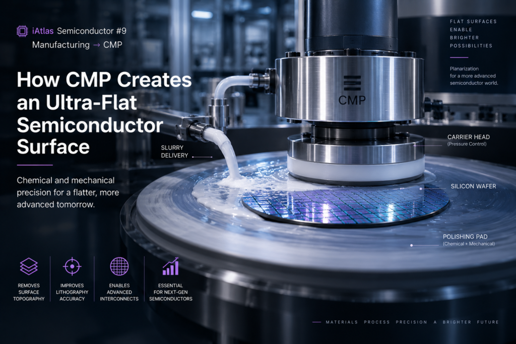
Chemical Mechanical Planarization (CMP) creates the extremely flat wafer surfaces required to manufacture modern semiconductor devices layer by layer.
Semiconductor fabrication repeatedly adds, patterns, etches, and modifies materials on a silicon wafer.
Each process can create small height differences across the surface.
If these differences continue to accumulate, later manufacturing steps become increasingly difficult to control.
Photolithography may lose focus. Thin films may become non-uniform. Interconnect structures may fail to align properly.
CMP solves this problem by combining chemical reactions with mechanical polishing to selectively remove material and restore surface flatness.
This makes CMP much more than a polishing process.
It is a critical enabling technology that allows semiconductor manufacturers to repeatedly build complex structures while maintaining the precision required for nanoscale devices.
Why Semiconductor Wafers Need Planarization
Imagine constructing a semiconductor device one layer at a time.
After deposition and etching, the surface is no longer perfectly flat.
Some regions are higher.
Others are lower.
As additional layers are formed, these height differences can accumulate.
A simplified sequence looks like:
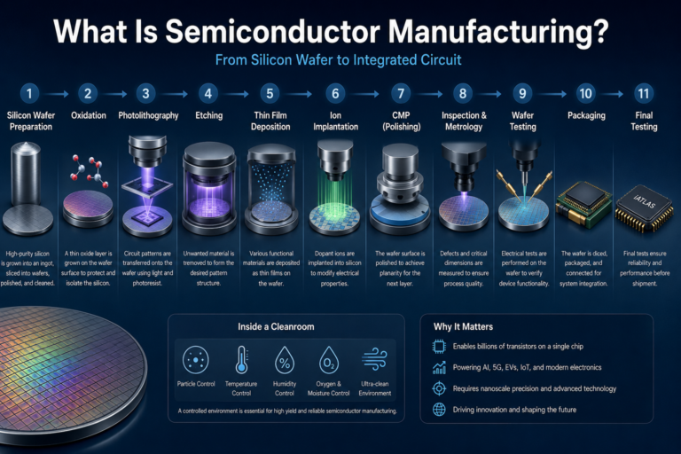
Deposition → Patterning → Etching → Uneven Surface → CMP → Flat Surface
The flat surface created by CMP provides a stable foundation for the next manufacturing cycle.
Without planarization, increasingly complex multilayer semiconductor structures would become extremely difficult to manufacture.
Why Surface Flatness Matters
Modern semiconductor manufacturing requires extraordinary dimensional control.
Photolithography systems must focus microscopic patterns onto the wafer surface.
If different areas of the wafer have significantly different heights, maintaining accurate focus becomes more difficult.
Poor surface planarity can contribute to:
- Lithography focus errors
- Pattern distortion
- Film thickness variation
- Overlay problems
- Interconnect defects
- Reduced manufacturing yield
CMP therefore helps maintain a controlled surface throughout semiconductor fabrication.
What Is Chemical Mechanical Planarization?
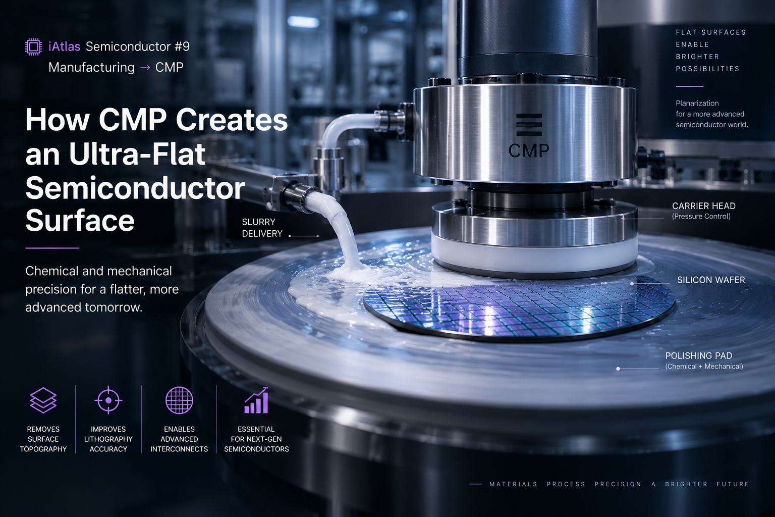
Chemical Mechanical Planarization removes material using two mechanisms simultaneously:
Chemical reaction + Mechanical abrasion
A chemical slurry interacts with the wafer surface and modifies the target material.
At the same time, the wafer is pressed against a rotating polishing pad.
The mechanical action of the pad and abrasive particles helps remove the chemically modified surface material.
The result is controlled material removal and improved surface planarity.
How CMP Works
A typical CMP process can be understood through several basic stages.
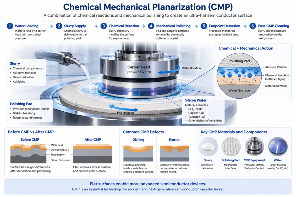
Step 1. Position the Wafer
The wafer is held by a carrier head.
The carrier head controls the wafer position and applies carefully regulated pressure during polishing.
Uniform pressure is important because uneven force can create different removal rates across the wafer.
Step 2. Supply the Slurry
A liquid CMP slurry is supplied onto the polishing pad.
The slurry typically contains:
- Chemical components
- Abrasive particles
- Deionized water
- Additives for process control
The exact formulation depends on the material being polished.
CMP slurries are engineered to control both chemical reactions and mechanical removal.
What Does CMP Slurry Do?
Slurry is one of the most important elements of CMP.
Its chemistry modifies the wafer surface so that the target material can be removed efficiently.
Abrasive particles then assist with mechanical removal.
Different CMP applications require different slurry chemistries.
The process may need to polish materials such as:
- Silicon dioxide
- Copper
- Tungsten
- Other dielectric or metallic films
The ideal slurry must remove the target material while minimizing damage to surrounding structures.
Step 3. Rotate the Pad and Wafer
During polishing, the wafer and polishing pad move relative to each other.
This motion distributes slurry across the wafer and produces controlled mechanical interaction between the wafer, slurry, and pad.
CMP performance depends on carefully controlled parameters such as:
- Rotation speed
- Downforce
- Slurry flow
- Pad condition
- Wafer temperature
- Polishing time
Small changes can affect removal rate and uniformity.
Step 4. Chemically Modify the Surface
The chemical components of the slurry react with the exposed wafer material.
Rather than relying only on aggressive mechanical grinding, CMP modifies the surface chemically so it can be removed in a more controlled manner.
This is one of the major differences between CMP and conventional mechanical polishing.
Step 5. Mechanically Remove Material
The polishing pad and slurry abrasives remove the chemically modified material.
Raised areas generally experience stronger polishing interaction than recessed areas.
Over time, the difference between high and low regions decreases.
The surface gradually becomes more planar.
Step 6. Detect the Endpoint
CMP must stop at the correct point.
Too little polishing leaves unwanted material behind.
Too much polishing may remove material that should remain.
Modern CMP systems therefore use process monitoring and endpoint detection to determine when the desired polishing condition has been reached.
Accurate endpoint control becomes increasingly important as film thicknesses decrease.
Step 7. Post-CMP Cleaning
Polishing leaves slurry particles, chemical residues, and removed material on the wafer.
These contaminants must be removed before subsequent processing.
A post-CMP cleaning step therefore follows polishing.
Effective cleaning is critical because remaining particles or metallic contamination can create defects later in the manufacturing process.
The Four Critical Elements of CMP
CMP performance can be understood through four closely connected components.
Wafer
The material and structure being planarized.
Slurry
Provides chemical reactions and abrasive action.
Polishing Pad
Creates mechanical contact and distributes slurry across the wafer.
CMP Equipment
Controls pressure, motion, slurry delivery, temperature, endpoint, and process uniformity.
Changing any one of these can affect the final surface.
CMP is therefore a tightly integrated process rather than a simple polishing operation.
What Is a CMP Polishing Pad?
The polishing pad provides the mechanical interface between the CMP equipment and the wafer.
Its surface characteristics influence:
- Slurry transport
- Contact behavior
- Removal rate
- Uniformity
- Defect generation
During repeated processing, the pad surface gradually changes.
This can alter polishing performance.
Maintaining consistent pad condition is therefore essential for stable high-volume manufacturing.
Why Pad Conditioning Is Needed
As CMP proceeds, slurry residues and removed materials can accumulate on the pad.
The pad surface may also become smoother.
This phenomenon can reduce polishing efficiency.
A pad conditioner is used to restore the desired pad surface condition.
Conditioning helps maintain:
- Surface texture
- Slurry distribution
- Removal rate
- Process repeatability
Pad condition is therefore an important part of CMP process control.
CMP Removal Rate
The removal rate describes how quickly material is removed from the wafer surface.
Higher removal rates can improve productivity, but speed alone is not the goal.
The process must balance:
- Removal rate
- Uniformity
- Selectivity
- Surface quality
- Defect control
A very fast CMP process that damages structures or produces non-uniform results would not be useful.
What Is CMP Selectivity?
Different materials may be exposed simultaneously during CMP.
The process may need to remove one material rapidly while preserving another.
Selectivity describes the relative removal rates of different materials.
Good selectivity is particularly important when a material underneath or adjacent to the target layer acts as a stopping layer.
Slurry chemistry and process conditions are therefore engineered for the specific material combination.
Oxide CMP
One major CMP application involves dielectric materials such as silicon dioxide.
Dielectric layers can become uneven after deposition over patterned structures.
CMP removes elevated regions and restores planarity before subsequent processing.
This helps provide a flatter surface for additional lithography, deposition, and interconnect fabrication.
Metal CMP
CMP is also essential for semiconductor metal interconnects.
Rather than simply patterning every metal layer through subtractive etching, some interconnect structures use a sequence in which trenches or vias are first created and then filled with metal.
Excess metal must then be removed from the wafer surface.
CMP performs this removal while leaving metal inside the desired recessed structures.
Copper CMP and the Damascene Process
Copper interconnect manufacturing provides one of the clearest examples of CMP.
A simplified sequence is:
Dielectric Deposition
↓
Trench / Via Formation
↓
Barrier & Copper Deposition
↓
Excess Copper
↓
CMP
↓
Copper Remains in Trenches and Vias
This approach is closely associated with the damascene process.
CMP removes excess copper from the upper surface while preserving copper inside the patterned interconnect structures.
Without highly controlled CMP, modern copper interconnect fabrication would be much more difficult.
What Are Dishing and Erosion?
CMP must remove material uniformly across many different pattern geometries.
Two important defects are dishing and erosion.
Dishing
Dishing occurs when material inside a recessed feature is polished too deeply, creating a concave surface.
This can occur in relatively wide metal structures.
Erosion
Erosion refers to excessive removal across regions containing dense patterns.
Both can change the intended geometry of semiconductor structures.
Controlling them requires careful optimization of slurry chemistry, pad behavior, pressure, and endpoint.
Scratches and Particle Defects
CMP involves direct mechanical interaction with the wafer.
As a result, particles can cause surface scratches.
Potential particle sources include:
- Slurry agglomerates
- Pad debris
- Removed wafer material
- Equipment contamination
Even microscopic scratches may damage sensitive structures.
Particle management and post-CMP cleaning are therefore major parts of CMP manufacturing.
Uniformity Across a 300 mm Wafer
A modern 300 mm wafer has a large surface area.
CMP must achieve highly consistent material removal from the center to the edge.
This is challenging because polishing pressure and relative motion can vary across the wafer.
Advanced carrier heads may therefore use multiple pressure zones to independently control different wafer regions.
The goal is to minimize within-wafer non-uniformity.
CMP and Process Integration
CMP does not operate independently.
The optimal polishing process depends on what happened before it and what will happen afterward.
For example:
- Deposition determines initial film thickness.
- Pattern density influences polishing behavior.
- CMP determines the surface available for the next lithography step.
- Cleaning determines whether residual contamination remains.
CMP must therefore be considered as part of the overall semiconductor process flow.
Why CMP Is Becoming More Challenging
Semiconductor structures continue to become smaller and more complex.
At the same time, manufacturers are introducing:
- New metals
- New dielectric materials
- More complex 3D structures
- Tighter thickness tolerances
- Smaller defect budgets
These changes make CMP increasingly demanding.
Removing only a few additional nanometers can influence device performance.
CMP therefore requires extremely precise control of material removal.
CMP in Advanced Logic Devices
Advanced logic technologies contain increasingly complex transistor and interconnect structures.
CMP can be used at multiple stages to provide the flat surfaces required for subsequent fabrication.
As structures move toward Gate-All-Around architectures and more sophisticated interconnect schemes, planarization remains important for maintaining dimensional control across many process layers.
CMP in Memory Manufacturing
Memory manufacturing also relies heavily on planarization.
DRAM and NAND devices contain repeated material layers and complex structures.
CMP may be used to manage surface topography during various manufacturing stages.
As 3D memory structures become taller and more complex, controlling wafer topography becomes increasingly challenging.
CMP Equipment and Process Control
Modern CMP equipment integrates several systems to maintain repeatable polishing conditions.
These may include:
- Carrier head pressure control
- Platen rotation
- Slurry delivery
- Pad conditioning
- Endpoint monitoring
- Temperature management
- Wafer handling
- Post-CMP cleaning integration
High-volume semiconductor manufacturing requires all of these systems to operate with tight repeatability.
CMP vs. Wafer Polishing
It is important to distinguish CMP during semiconductor device fabrication from the wafer polishing discussed earlier in the Silicon Wafer Manufacturing article.
Wafer manufacturing polishing prepares the original silicon wafer before semiconductor fabrication begins.
CMP, in contrast, occurs repeatedly during device fabrication to planarize deposited and patterned material layers.
| Wafer Polishing | CMP |
|---|---|
| Performed during wafer manufacturing | Performed during device fabrication |
| Creates initial mirror-quality silicon surface | Restores planarity between process layers |
| Primarily prepares the substrate | Enables multilayer device construction |
| Before wafer enters the fab | Repeated during semiconductor processing |
This distinction is important because the two processes serve different manufacturing purposes.
The Future of CMP
As semiconductor manufacturing advances, CMP must provide increasingly precise control.
Future development areas include:
- Lower defectivity
- Better endpoint detection
- Advanced slurry chemistry
- Improved pad materials
- More precise pressure control
- New metal CMP processes
- Advanced 3D device planarization
- Improved post-CMP cleaning
- Data-driven process control
Even as semiconductor architectures change, the need for controlled surface planarity remains fundamental.
Key Takeaways
- Chemical Mechanical Planarization (CMP) creates flat surfaces during semiconductor device fabrication.
- CMP combines chemical surface reactions with mechanical polishing.
- Slurry, polishing pads, carrier pressure, and endpoint control are key process elements.
- CMP is required because repeated deposition and patterning create uneven wafer topography.
- Copper CMP is essential to damascene interconnect fabrication.
- Dishing, erosion, scratches, particles, and non-uniformity are major CMP challenges.
- Post-CMP cleaning removes slurry and polishing residues before subsequent processing.
- CMP differs from the polishing used to manufacture the original silicon wafer.
- Advanced semiconductor structures require increasingly precise planarization.
Frequently Asked Questions
What is CMP in semiconductor manufacturing?
Chemical Mechanical Planarization is a process that combines chemical reactions and mechanical polishing to remove material and create a flat wafer surface during semiconductor device fabrication.
Why is CMP necessary?
Repeated deposition, lithography, and etching create surface height differences. CMP removes this topography so subsequent process layers can be fabricated accurately.
What is CMP slurry?
CMP slurry is a liquid containing chemical components, abrasive particles, water, and process additives. It helps chemically modify and mechanically remove target materials.
What is the difference between CMP and wafer polishing?
Wafer polishing prepares the initial silicon wafer before device fabrication, while CMP is repeatedly used during semiconductor manufacturing to planarize deposited and patterned layers.
What are dishing and erosion in CMP?
Dishing is excessive polishing within a recessed feature, while erosion is excessive material removal across patterned regions. Both can alter intended device geometry.
📖 Semiconductor Learning Path
Previous
💻 Semiconductor #8 | How Ion Implantation Engineers Silicon at the Atomic Level
⬇️
Current
💻 Semiconductor #9 | How CMP Creates an Ultra-Flat Semiconductor Surface
⬇️
Next
💻 Semiconductor #10 | How Semiconductor Inspection & Metrology Find Nanometer-Scale Defects
📚 Continue Reading
- 💻 Semiconductor #5 | How Photolithography Creates Billions of Transistors
- 💻 Semiconductor #6 | How Plasma Etching Shapes Semiconductor Devices
- 💻 Semiconductor #7 | How Thin Film Deposition Builds Semiconductor Devices Layer by Layer
- 💻 Semiconductor #8 | How Ion Implantation Engineers Silicon at the Atomic Level
- 💻 Semiconductor #10 | How Semiconductor Inspection & Metrology Find Nanometer-Scale Defects
References
Recommended primary sources for this article:
🔷 About iAtlas
iAtlas is an independent publication covering batteries, semiconductors, OLED, advanced materials, AI, and global industrial trends.
We transform complex industrial developments into clear, reliable, and easy-to-understand insights.
Whether you’re following today’s industry news or building long-term expertise, iAtlas helps you understand not only what happened, but why it matters.
Technology creates change.
Insight creates opportunity.
— iAtlas