Explore All Semiconductor Articles
-
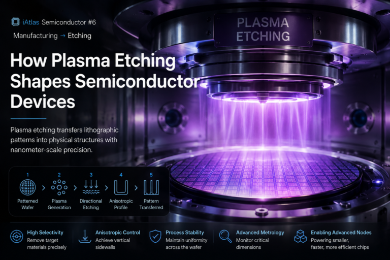
How Plasma Etching Shapes Semiconductor Devices
π» iAtlas Semiconductor #6 | π Manufacturing β Etching Introduction Plasma etching transforms the patterns created by photolithography into physical structures on a semiconductor wafer. Photolithography determines where a feature should be formed. Etching determines where material should be removed. This distinction is fundamental to semiconductor manufacturing. After a photoresist pattern is created on the…
-
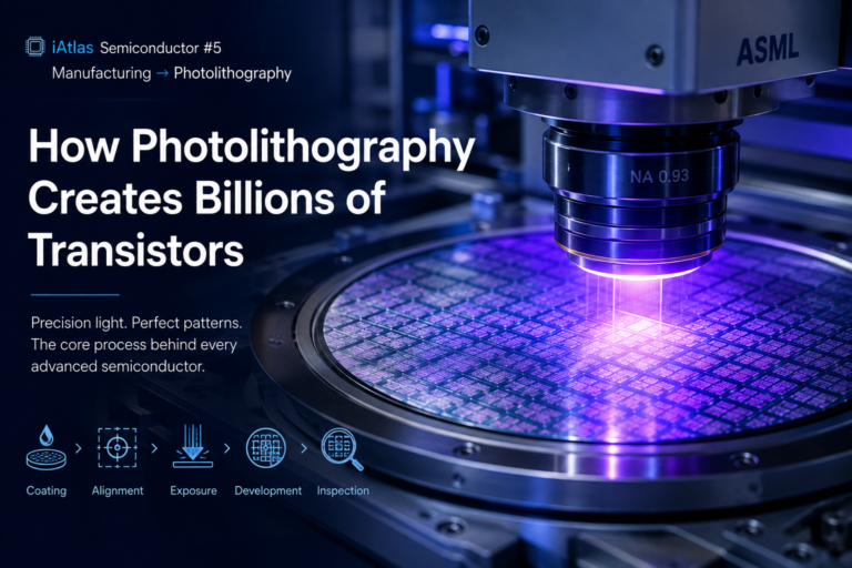
How Photolithography Creates Billions of Transistors
π» iAtlas Semiconductor #5 | π Manufacturing β Photolithography Introduction Every modern semiconductor chip contains millionsβor even billionsβof microscopic transistors. Creating these tiny structures requires an extraordinary level of precision. Features measuring only a few nanometers must be transferred accurately onto a silicon wafer, layer after layer, without deviation. The manufacturing process responsible for transferring…
-
Silicon Wafer Manufacturing: Cutting, Lapping, and Polishing Explained
π» iAtlas Semiconductor #4 | π Fundamentals β Wafer Manufacturing Introduction Silicon wafer manufacturing begins after the Czochralski Process produces a single-crystal silicon ingot. Before integrated circuits can be built, the ingot must be transformed into ultra-flat, mirror-like silicon wafers with extremely tight dimensional tolerances. This transformation involves several precision manufacturing processes, including slicing, edge…
-
How the Czochralski Process Creates Single-Crystal Silicon
π» iAtlas Semiconductor #3 | π Fundamentals β Crystal Growth Introduction Every semiconductor chip begins with silicon, but not just any silicon. Modern integrated circuits require an extremely pure and perfectly ordered crystal structure capable of supporting billions of microscopic transistors. Before a silicon wafer can enter photolithography, etching, or deposition, it must first be…
-
Why Silicon Wafers Are the Foundation of Modern Chips
π» iAtlas Semiconductor #2 | π Fundamentals β Silicon Wafer Introduction Before a semiconductor chip can contain billions of transistors, it needs a physical foundation capable of supporting hundreds of highly precise manufacturing steps. That foundation is the silicon wafer. A silicon wafer may appear to be a simple circular disc, but its crystal quality,…
-
What Is Semiconductor Manufacturing?
π» iAtlas Semiconductor #1 | π Fundamentals β Manufacturing Overview Introduction Semiconductor manufacturing is the highly advanced process of transforming a silicon wafer into thousands of integrated circuits (ICs) through hundreds of precisely controlled fabrication steps. Every smartphone, AI server, electric vehicle, medical device, and industrial robot relies on semiconductor chips produced using this manufacturing…

Structured industrial knowledge for engineers, researchers, students, and professionals.
Explore
Industries
Industry Briefing
Resources
Learn
Atlas Library
Learning Paths
Engineering Fundamentals
About
About iAtlas
Contact
Editorial Policy
Legal
Privacy Policy
Terms of Use
Β© 2026 iAtlas. All rights reserved.