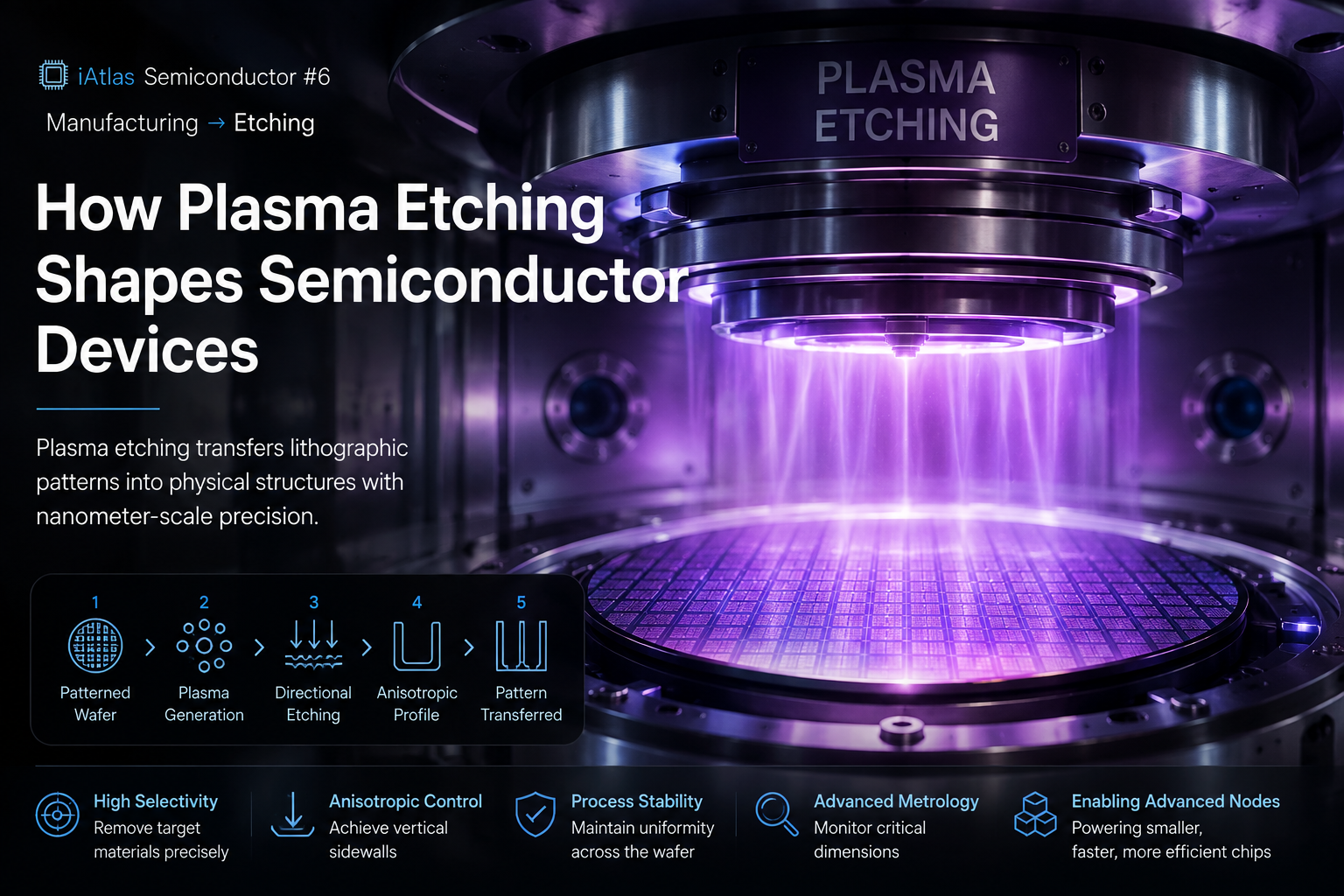
How Plasma Etching Shapes Semiconductor Devices
💻 iAtlas Semiconductor #6 | 📘 Manufacturing → Etching
Introduction
Plasma etching transforms the patterns created by photolithography into physical structures on a semiconductor wafer.
Photolithography determines where a feature should be formed. Etching determines where material should be removed.
This distinction is fundamental to semiconductor manufacturing.
After a photoresist pattern is created on the wafer, selected areas of an underlying material must be removed with extraordinary precision. Modern semiconductor structures may be only a few nanometers wide while extending vertically through multiple material layers.
To create these structures, advanced fabs rely heavily on plasma-based dry etching.
Plasma etching combines chemistry, ionized gases, vacuum technology, RF power, and precise process control to selectively remove material from microscopic regions of a wafer.
Without this process, the patterns created by lithography could never become functional transistors, contacts, interconnects, or memory structures.
From Pattern to Physical Structure
Consider the relationship between photolithography and etching.
The simplified sequence is:
Film Deposition → Photoresist → Photolithography → Etching → Photoresist Removal
First, a material layer is formed on the wafer.
Photoresist is then coated and patterned using photolithography. The remaining resist protects selected areas of the underlying material.
Etching removes material from the exposed regions while leaving protected regions largely intact.
After the photoresist is removed, the underlying layer contains the desired physical pattern.
This sequence is repeated many times during semiconductor fabrication.
Why Plasma Etching Matters
As semiconductor features become smaller, simply removing material is not enough.
The process must remove the right material, in the right location, to the right depth, with the right profile.
Modern etching processes therefore require control over:
- Etch rate
- Selectivity
- Anisotropy
- Critical Dimension (CD)
- Sidewall profile
- Uniformity
- Endpoint
- Surface damage
- Defect generation
A small variation in any of these parameters can affect transistor performance or manufacturing yield.
Wet Etching vs. Dry Etching
Semiconductor manufacturing uses two major approaches to material removal: wet etching and dry etching.
| Wet Etching | Dry Etching |
|---|---|
| Uses liquid chemicals | Uses reactive gases or plasma |
| Often isotropic | Can achieve highly anisotropic profiles |
| Relatively simple equipment | More complex vacuum equipment |
| High throughput for some applications | Excellent dimensional control |
| Useful for cleaning and selective removal | Essential for advanced pattern transfer |
Wet etching remains important in semiconductor manufacturing.
However, advanced semiconductor structures increasingly depend on dry plasma etching because it provides much greater control over vertical profiles.
What Is Plasma?
A plasma is an ionized gas containing a mixture of:
- Electrons
- Ions
- Neutral atoms
- Molecules
- Reactive radicals
In semiconductor etching equipment, process gases are introduced into a vacuum chamber and energized using electromagnetic energy, commonly RF power.
The resulting plasma generates highly reactive species capable of interacting with materials on the wafer surface.
These interactions allow material to be removed through a combination of chemical reactions and physical ion bombardment.
How Plasma Etching Works
A simplified plasma etching process can be divided into several stages.
Step 1. Load the Wafer
The patterned wafer enters the etch chamber through an automated vacuum transfer system.
The wafer is placed onto a precisely controlled electrostatic chuck or wafer stage.
Temperature control is critical because reaction rates and profile characteristics can change with wafer temperature.
Step 2. Create a Vacuum
The chamber pressure is reduced significantly below atmospheric pressure.
Vacuum conditions allow engineers to precisely control gas composition, particle collisions, plasma behavior, and reaction conditions.
Stable pressure is essential for repeatable etching.
Step 3. Introduce Process Gases
Specific gases are introduced depending on the material being etched.
Different material systems require different chemistries.
Examples may include fluorine-, chlorine-, or bromine-based chemistries depending on the application.
The goal is to generate reactive species that interact selectively with the target material.
Step 4. Generate Plasma
RF energy is applied to the process gas.
Energetic electrons collide with gas molecules, creating ions and reactive radicals.
The chamber now contains a plasma capable of interacting with the exposed wafer surface.
Step 5. Remove Material
Reactive species reach the wafer surface and react with exposed materials.
At the same time, positively charged ions may be accelerated toward the wafer.
This combination of chemical reaction and directional ion bombardment allows material to be removed with high precision.
The photoresist or another hard mask protects areas that should remain.
Step 6. Detect the Endpoint
The etching process must stop at the correct moment.
Stopping too early can leave unwanted material behind.
Stopping too late can damage the layer underneath.
Modern systems therefore use endpoint detection techniques to determine when the target layer has been sufficiently removed.
Step 7. Remove the Wafer
After etching is complete, plasma generation stops and remaining process gases are removed.
The wafer is transferred out of the chamber for subsequent processing.
Depending on the process, the remaining photoresist or hard mask may then be stripped.
Why Directionality Matters
One of the most important concepts in advanced etching is anisotropy.
An isotropic process removes material in multiple directions.
This can cause lateral undercutting beneath the mask.
An anisotropic process removes material primarily in the vertical direction.
For modern semiconductor manufacturing, vertical control is critical because circuit patterns are extremely small and densely packed.
A highly directional etch can produce narrow trenches with relatively vertical sidewalls while preserving the intended lateral dimensions.
Isotropic vs. Anisotropic Etching
Imagine a mask opening above a material layer.
With isotropic etching, material is removed downward and sideways.
The resulting structure may become wider underneath the mask.
With anisotropic etching, material removal is concentrated primarily downward.
This allows the etched structure to more closely reproduce the dimensions defined by photolithography.
As semiconductor structures become increasingly three-dimensional, anisotropic control becomes even more important.
Reactive Ion Etching (RIE)
Reactive Ion Etching, commonly known as RIE, combines chemical reactions with directional ion bombardment.
Reactive radicals contribute chemical selectivity, while energetic ions help control the direction of material removal.
This combination provides significantly better profile control than many purely chemical processes.
RIE has therefore become an important foundation of modern semiconductor pattern transfer.
ICP Etching
More advanced plasma systems often use Inductively Coupled Plasma (ICP) technology.
ICP systems can generate high-density plasma while allowing greater independent control over plasma generation and ion energy at the wafer.
This provides process engineers with additional flexibility to optimize:
- Etch rate
- Selectivity
- Sidewall profile
- Plasma density
- Ion energy
- Wafer damage
Such control is especially valuable for demanding nanoscale structures.
What Is Etch Selectivity?
Etch selectivity describes how much faster one material is removed compared with another.
For example, an etching process may need to remove a dielectric layer while minimizing removal of the mask or underlying material.
High selectivity helps protect:
- Photoresist
- Hard masks
- Stop layers
- Underlying films
This becomes increasingly challenging as semiconductor structures become thinner and more complex.
Why Critical Dimension Control Matters
The dimensions created during lithography must survive the etching process.
If a 20 nm pattern is defined in photoresist but becomes significantly wider or narrower after etching, the resulting device may not function as designed.
Etch processes therefore require precise Critical Dimension (CD) control.
Important factors include:
- Plasma chemistry
- Chamber pressure
- RF power
- Wafer temperature
- Mask properties
- Etch time
Modern equipment continuously controls these parameters to maintain repeatability across the wafer and from wafer to wafer.
Sidewall Profile Control
Advanced semiconductor structures are not always simple vertical trenches.
Engineers may require:
- Vertical profiles
- Tapered profiles
- Rounded features
- High-aspect-ratio structures
- Extremely deep and narrow holes
The ideal profile depends on the device being manufactured.
For this reason, plasma etching is not simply a removal process—it is a three-dimensional structure-engineering process.
High-Aspect-Ratio Etching
One of the biggest challenges in modern semiconductor manufacturing is creating structures that are extremely narrow but very deep.
This is known as a high-aspect-ratio structure.
The challenge is especially important in technologies such as:
- 3D NAND
- DRAM
- Advanced interconnects
- MEMS
- Through-silicon structures
As 3D NAND stacks increase in layer count, etching must penetrate through increasingly thick multilayer structures while maintaining accurate profiles.
This makes high-aspect-ratio plasma etching one of the most sophisticated processes in semiconductor manufacturing.
Plasma Etching in 3D NAND
3D NAND provides a particularly clear example of why advanced etching matters.
Unlike traditional planar memory, 3D NAND stacks memory cells vertically.
Manufacturers must create extremely deep channel holes through many alternating material layers.
These holes must maintain tight dimensional control from the top of the stack to the bottom.
Challenges include:
- Profile distortion
- Sidewall roughness
- Etch non-uniformity
- Aspect-ratio-dependent etching
- Mask erosion
As layer counts increase, etch technology becomes a major factor determining how far 3D NAND scaling can continue.
Plasma Etching and Advanced Logic
Logic semiconductor architectures are also becoming increasingly three-dimensional.
The industry has progressed from planar transistors to FinFETs and now toward Gate-All-Around (GAA) structures.
These architectures require highly selective removal of specific materials while preserving extremely small neighboring structures.
Advanced etching therefore plays a critical role in forming:
- Fins
- Nanosheets
- Gate structures
- Contacts
- Interconnect features
As device architecture becomes more complex, atomic-scale process control becomes increasingly important.
Atomic Layer Etching
One emerging approach is Atomic Layer Etching (ALE).
Instead of continuously removing material, ALE uses sequential, self-limiting surface reactions to remove extremely small amounts of material during each cycle.
A simplified concept is:
Surface Modification → Controlled Removal → Repeat
This approach can provide exceptional control over material removal.
ALE is particularly attractive for advanced devices where conventional continuous plasma etching may remove too much material or cause excessive damage.
Chamber Cleanliness and Process Stability
Plasma etching occurs inside a highly controlled vacuum chamber.
Over time, reaction by-products can accumulate on chamber surfaces.
These deposits may alter plasma conditions or generate particles.
Equipment therefore requires careful chamber conditioning and cleaning to maintain process repeatability.
Stable semiconductor production depends not only on the plasma itself but also on:
- Chamber materials
- Gas delivery
- Vacuum performance
- Temperature control
- RF stability
- Contamination management
This is why etch equipment is among the most sophisticated systems inside a semiconductor fab.
Why Etching Affects Yield
An etch process can appear successful while still introducing microscopic problems.
Potential defects include:
- Residue
- Under-etch
- Over-etch
- Sidewall damage
- Profile deformation
- Mask erosion
- Plasma-induced damage
- Particles
Because modern devices contain billions of features, even a very low defect rate can affect a significant number of dies.
Process uniformity across the entire wafer is therefore essential.
The Future of Plasma Etching
Semiconductor scaling is changing the role of etching.
The industry is moving beyond simply creating smaller two-dimensional patterns toward engineering complex three-dimensional structures.
Future development areas include:
- Atomic Layer Etching
- Higher-selectivity processes
- Lower plasma damage
- Advanced high-aspect-ratio etching
- Improved chamber control
- AI-assisted process optimization
- More precise endpoint detection
- Better control for GAA and 3D memory structures
As semiconductor architectures become increasingly three-dimensional, plasma etching will remain one of the technologies that determines how far device scaling can progress.
Key Takeaways
- Plasma etching transfers lithographic patterns into physical semiconductor structures.
- Photolithography defines where a feature belongs, while etching removes material to create that feature.
- Dry plasma etching provides the directional control required for advanced semiconductor manufacturing.
- Reactive Ion Etching combines chemical reactions with directional ion bombardment.
- Selectivity, anisotropy, Critical Dimension, uniformity, and sidewall profile are key etch parameters.
- High-aspect-ratio etching is increasingly important for 3D NAND and other three-dimensional devices.
- Advanced logic architectures such as GAA require extremely precise and selective etching.
- Atomic Layer Etching may provide increasingly fine control as semiconductor dimensions continue to shrink.
Frequently Asked Questions
What is plasma etching in semiconductor manufacturing?
Plasma etching is a dry material-removal process that uses reactive plasma species and ion bombardment to transfer lithographic patterns into semiconductor material layers.
What is the difference between wet etching and plasma etching?
Wet etching uses liquid chemicals and is often isotropic, while plasma etching uses reactive gases under vacuum and can provide highly directional material removal.
Why is anisotropic etching important?
Anisotropic etching minimizes sideways material removal, allowing narrow semiconductor structures with precisely controlled dimensions and sidewalls.
What is Reactive Ion Etching?
Reactive Ion Etching combines chemical reactions with directional ion bombardment to achieve controlled and anisotropic material removal.
Why is plasma etching important for 3D NAND?
3D NAND requires deep, narrow structures to be etched through many stacked material layers. Maintaining the correct profile throughout these high-aspect-ratio structures requires highly advanced plasma etching technology.
📖 Semiconductor Learning Path
Previous: 💻 Semiconductor #5 | How Photolithography Creates Billions of Transistors
⬇️
Current: 💻 Semiconductor #6 | How Plasma Etching Shapes Semiconductor Devices
⬇️
Next: 💻 Semiconductor #7 | How Thin Film Deposition Builds Semiconductor Devices Layer by Layer
📚 Continue Reading
- 💻 Semiconductor #4 | Wafer Manufacturing: From Silicon Ingot to Wafer
- 💻 Semiconductor #5 | How Photolithography Creates Billions of Transistors
- 💻 Semiconductor #7 | How Thin Film Deposition Builds Semiconductor Devices Layer by Layer
- 💻 Semiconductor #8 | How Ion Implantation Engineers Silicon at the Atomic Level
- 💻 Semiconductor #9 | How CMP Creates an Ultra-Flat Semiconductor Surface
References
For this article, I recommend using official technical sources from:
🔷 About iAtlas
iAtlas is an independent publication covering batteries, semiconductors, OLED, advanced materials, AI, and global industrial trends.
We transform complex industrial developments into clear, reliable, and easy-to-understand insights.
Whether you’re following today’s industry news or building long-term expertise, iAtlas helps you understand not only what happened, but why it matters.
Technology creates change.
Insight creates opportunity.
— iAtlas