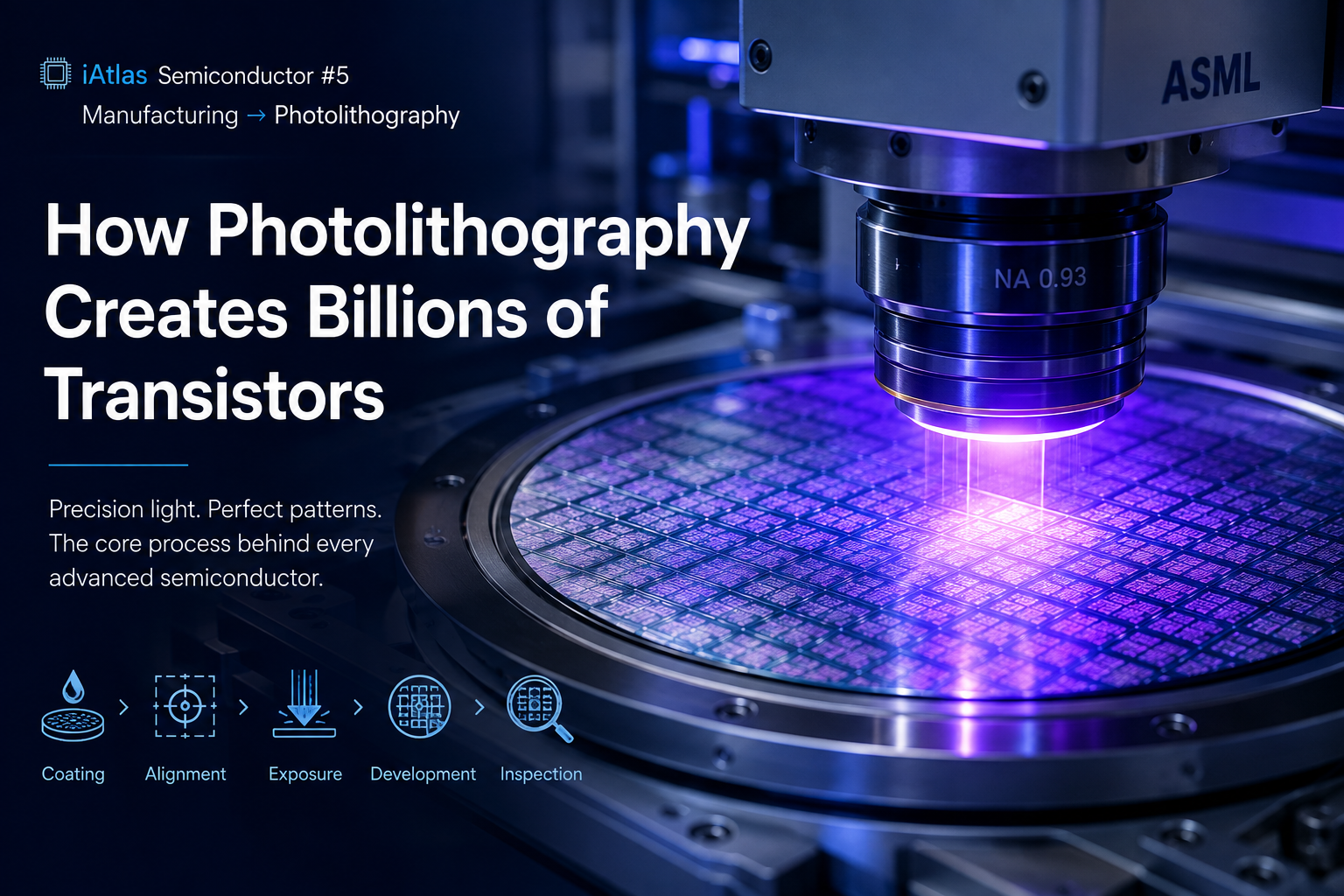
How Photolithography Creates Billions of Transistors
💻 iAtlas Semiconductor #5 | 📘 Manufacturing → Photolithography
Introduction
Every modern semiconductor chip contains millions—or even billions—of microscopic transistors.
Creating these tiny structures requires an extraordinary level of precision. Features measuring only a few nanometers must be transferred accurately onto a silicon wafer, layer after layer, without deviation.
The manufacturing process responsible for transferring these intricate circuit patterns is photolithography.
Often compared to photography because it uses light to create patterns, photolithography is actually one of the most advanced manufacturing technologies ever developed. It combines optics, chemistry, precision mechanics, and automation to define the circuitry that powers smartphones, AI processors, memory chips, and countless other electronic devices.
Without photolithography, modern semiconductor manufacturing simply would not be possible.
Why Photolithography Matters
Integrated circuits are built by repeating hundreds of manufacturing steps.
At the heart of nearly every step lies one common requirement: accurately defining where materials should remain and where they should be removed.
Photolithography provides this capability by transferring circuit patterns from a photomask onto a photosensitive material called photoresist.
Because every transistor, interconnect, and contact opening depends on this process, photolithography largely determines:
- Feature size
- Pattern accuracy
- Overlay precision
- Device performance
- Manufacturing yield
As semiconductor technology advances toward smaller process nodes, photolithography becomes increasingly critical.
What Is Photolithography?
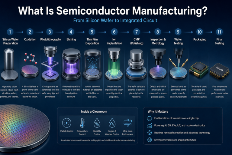
Photolithography is a pattern-transfer process that uses ultraviolet light to project microscopic circuit designs onto a photoresist-coated silicon wafer.
Rather than creating circuits directly, photolithography defines where subsequent manufacturing processes—such as etching, ion implantation, or deposition—will occur.
The process is repeated many times throughout semiconductor fabrication, with each layer requiring extremely accurate alignment to the layers already formed beneath it.
Modern advanced chips may require more than 60 photolithography cycles during fabrication.
The Basic Photolithography Flow
The simplified manufacturing sequence includes:
- Wafer Cleaning
- Photoresist Coating
- Soft Bake
- Mask Alignment
- Exposure
- Post-Exposure Bake
- Development
- Inspection
Each stage contributes to creating precise circuit patterns with nanometer-scale accuracy.
Step 1. Wafer Cleaning
Before applying photoresist, the wafer surface must be free of particles, organic residue, and moisture.
Even a single microscopic particle can distort the circuit pattern and reduce manufacturing yield.
Cleaning therefore ensures excellent adhesion between the wafer and the photoresist layer.
Step 2. Photoresist Coating
A liquid photoresist is dispensed onto the center of the wafer.
The wafer then spins at high speed, spreading the resist into an extremely uniform thin film.
This technique, known as spin coating, produces a resist layer whose thickness is carefully controlled according to the manufacturing process.
Step 3. Soft Bake
After coating, the photoresist still contains solvents.
The wafer is gently heated to remove excess solvent and improve the stability of the resist before exposure.
This step enhances coating uniformity and prepares the resist for accurate pattern transfer.
Step 4. Mask Alignment
A photomask contains the circuit design for one specific layer of the integrated circuit.
Before exposure begins, the photolithography system aligns the mask with alignment marks already present on the wafer.
Modern lithography systems achieve overlay accuracy measured in only a few nanometers.
Accurate alignment is essential because semiconductor devices are built layer upon layer.
Step 5. Exposure
Ultraviolet light passes through—or is reflected by—the photomask and projects the circuit pattern onto the photoresist.
Depending on the photoresist chemistry:
- Positive photoresist becomes soluble where exposed to light.
- Negative photoresist becomes insoluble where exposed.
Exposure is the defining step of photolithography, determining the size and accuracy of every circuit feature.
Step 6. Post-Exposure Bake
Following exposure, the wafer is heated again.
This bake stabilizes the chemical reactions initiated by ultraviolet light and improves pattern fidelity.
Proper temperature control helps reduce defects such as standing waves and line-edge roughness.
Step 7. Development
The wafer is immersed in or sprayed with a developer solution.
Depending on the photoresist type, either the exposed or unexposed regions dissolve away.
After development, the desired circuit pattern remains on the wafer surface.
This patterned photoresist now acts as a temporary protective layer for later manufacturing processes.
Step 8. Inspection
Optical inspection systems examine the wafer to verify:
- Pattern dimensions
- Critical Dimension (CD)
- Overlay accuracy
- Pattern defects
- Particle contamination
Early defect detection helps improve manufacturing yield and reduces downstream processing costs.
Positive vs. Negative Photoresist
| Positive Photoresist | Negative Photoresist |
|---|---|
| Exposed areas dissolve | Exposed areas remain |
| Higher resolution | Better mechanical strength |
| Widely used in advanced semiconductor manufacturing | Often used for MEMS and specialty applications |
Today, positive photoresists dominate leading-edge semiconductor production due to their superior resolution.
Why Resolution Is So Important
The resolution of a photolithography system determines the smallest feature that can be printed onto the wafer.
Smaller features enable:
- Higher transistor density
- Faster processors
- Lower power consumption
- Greater memory capacity
As feature sizes continue to shrink, improvements in optics, photoresists, and exposure systems become increasingly important.
From DUV to EUV Lithography
Photolithography technology has evolved significantly over the past several decades.
DUV (Deep Ultraviolet)
- Uses 193 nm wavelength light
- Mature and widely adopted
- Multiple patterning required for advanced nodes
EUV (Extreme Ultraviolet)
- Uses 13.5 nm wavelength light
- Enables smaller feature sizes
- Reduces the need for multiple patterning
- Essential for leading-edge logic and memory manufacturing
EUV lithography represents one of the most significant advances in semiconductor manufacturing.
Why Photolithography Determines Yield
Photolithography errors can propagate throughout the manufacturing process.
Common issues include:
- Overlay errors
- Pattern collapse
- Focus variation
- Exposure dose errors
- Line-edge roughness
- Particle defects
Because every subsequent process depends on accurate pattern placement, lithography quality has a major influence on overall manufacturing yield.
Looking Ahead
As semiconductor technology moves toward increasingly advanced process nodes, photolithography continues to evolve.
Future developments include:
- High-NA EUV lithography
- Improved photoresists
- Computational lithography
- AI-assisted process optimization
- Higher overlay accuracy
- Faster inspection systems
These innovations will enable even smaller transistor dimensions and more powerful semiconductor devices.
Key Takeaways
- Photolithography transfers microscopic circuit patterns onto silicon wafers using ultraviolet light.
- The process includes coating, baking, alignment, exposure, development, and inspection.
- Accurate lithography is essential for transistor scaling and manufacturing yield.
- Positive photoresists dominate advanced semiconductor production.
- EUV lithography enables next-generation semiconductor manufacturing by supporting extremely small feature sizes.
📖 Semiconductor Learning Path
Previous: 💻 Semiconductor #4 | Wafer Manufacturing: From Silicon Ingot to Wafer
⬇️
Current: 💻 Semiconductor #5 | How Photolithography Creates Billions of Transistors
⬇️
Next: 💻 Semiconductor #6 | How Plasma Etching Shapes Semiconductor Devices
📚 Continue Reading
- 💻 Semiconductor #4 | Wafer Manufacturing: From Silicon Ingot to Wafer
- 💻 Semiconductor #6 | How Plasma Etching Shapes Semiconductor Devices
- 💻 Semiconductor #7 | Thin Film Deposition Explained
- 💻 Semiconductor #8 | Ion Implantation Explained
- 💻 Semiconductor #9 | Chemical Mechanical Planarization (CMP) Explained
References
🔷 About iAtlas
iAtlas is an independent publication covering batteries, semiconductors, OLED, advanced materials, AI, and global industrial trends.
We transform complex industrial developments into clear, reliable, and easy-to-understand insights.
Whether you’re following today’s industry news or building long-term expertise, iAtlas helps you understand not only what happened, but why it matters.
Technology creates change.
Insight creates opportunity.
— iAtlas