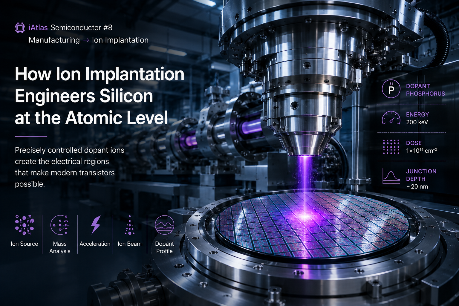
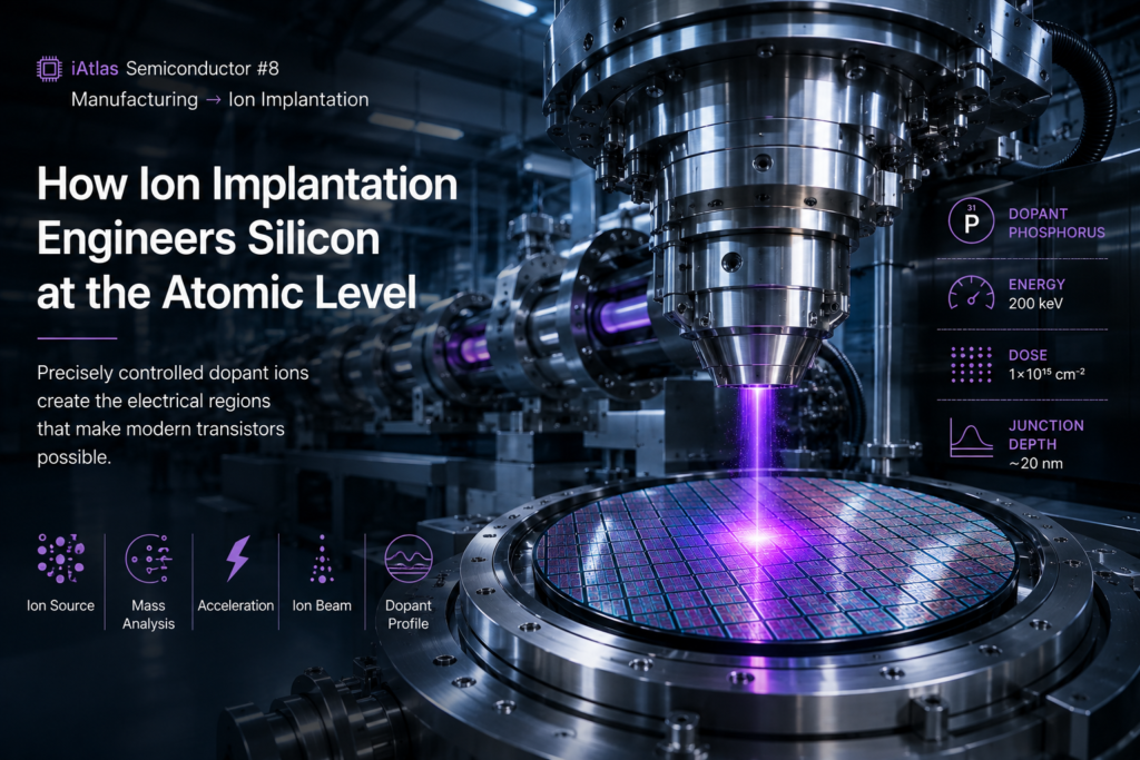
How Ion Implantation Engineers Silicon at the Atomic Level
💻 iAtlas Semiconductor #8 | 📘 Manufacturing → Ion Implantation
Introduction
Ion implantation modifies the electrical properties of semiconductor materials by introducing precisely controlled amounts of dopant atoms into selected regions of a silicon wafer.
A pure silicon crystal alone cannot provide all the electrical characteristics required to build billions of transistors.
Engineers must create regions with different electrical properties and carefully control where those regions begin, how deep they extend, and how many dopant atoms they contain.
Ion implantation makes this possible.
The process accelerates electrically charged dopant ions toward a wafer and embeds them beneath its surface.
By controlling the ion species, energy, dose, and implantation angle, semiconductor manufacturers can engineer the electrical characteristics of silicon with remarkable precision.
Why Semiconductor Silicon Needs Doping
Silicon is a semiconductor, meaning its electrical conductivity lies between that of a conductor and an insulator.
Its electrical behavior can be intentionally modified through doping.
Doping introduces small amounts of impurity atoms into the silicon crystal.
Depending on the dopant, the resulting material can become:
- n-type semiconductor
- p-type semiconductor
This ability to create regions with different electrical properties is fundamental to transistor operation.
Without precisely controlled doping, modern CMOS devices could not function.
What Is Ion Implantation?
Ion implantation is a semiconductor manufacturing process in which dopant atoms are ionized, accelerated, separated, and directed toward a wafer.
A simplified process flow is:
Dopant Source → Ionization → Acceleration → Mass Selection → Beam Control → Wafer Implantation
The energetic ions penetrate the wafer surface and become embedded within the silicon crystal.
Their final depth depends largely on the energy applied during implantation.
The total number of implanted ions is controlled by the dose.
Together, energy and dose allow engineers to control both the location and concentration of dopants.
From Photolithography to Ion Implantation
Ion implantation does not normally modify the entire wafer uniformly.
Instead, selected regions must be exposed while other regions remain protected.
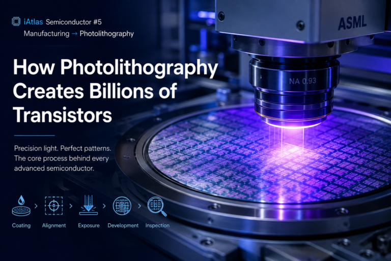
This is where photolithography becomes important again.
A simplified sequence is:
Photoresist Coating → Photolithography → Pattern Formation → Ion Implantation → Resist Removal
Photoresist or another masking material protects regions where dopants should not enter.
Ions penetrate exposed areas.
The mask therefore determines the lateral location of implantation, while implantation conditions determine the depth and concentration.
This combination allows extremely precise electrical regions to be created across a semiconductor wafer.
How an Ion Implanter Works
An ion implantation system contains several major functional sections.
Although equipment designs vary, the basic process can be understood through the following stages.
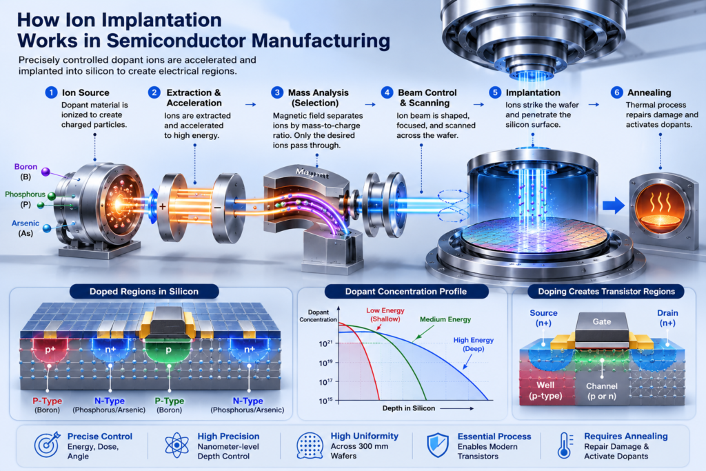
Step 1. Generate Dopant Ions
The process begins with a dopant source.
Materials containing the desired dopant element are introduced into an ion source.
Common semiconductor dopants include:
- Boron
- Phosphorus
- Arsenic
Energy is applied to ionize the source material, producing electrically charged particles.
These ions can then be manipulated using electric and magnetic fields.
Step 2. Extract and Accelerate the Ions
The charged ions are extracted from the source and accelerated.
Electric fields provide the ions with kinetic energy.
The selected implantation energy strongly influences how deeply the ions penetrate the wafer.
In general:
Higher Energy → Deeper Implantation
Lower Energy → Shallower Implantation
This relationship allows engineers to create different dopant profiles for different device structures.
Step 3. Select the Desired Ion Species
The ion source may produce several types of charged particles.
Only the required dopant ions should reach the wafer.
Ion implantation equipment therefore uses mass-analysis systems to separate ions according to their mass-to-charge ratio.
A magnetic field bends the path of the ion beam.
Different ion species follow different trajectories.
Only the desired ions are allowed to continue through the beamline.
This helps ensure that the correct dopant reaches the wafer.
Step 4. Control the Ion Beam
After mass selection, the ion beam must be precisely controlled.
Important parameters include:
- Beam current
- Beam shape
- Energy
- Uniformity
- Position
- Angle
The system may scan the beam across the wafer or move the wafer relative to the beam.
The goal is to achieve a carefully controlled implantation dose across the required wafer area.
Step 5. Implant the Wafer
The accelerated ions strike the wafer surface and penetrate into the silicon.
As they travel through the crystal, they collide with silicon atoms and gradually lose energy.
Eventually, the implanted ions come to rest beneath the surface.
The resulting dopant distribution is not a perfectly sharp layer.
Instead, it forms a depth profile determined by factors such as:
- Ion species
- Implantation energy
- Wafer material
- Crystal orientation
This profile must be carefully engineered for the intended device structure.
Step 6. Monitor the Dose
The implantation dose represents the number of ions delivered to a given wafer area.
Dose is one of the most important process parameters because it influences the resulting dopant concentration.
Too little dopant may fail to produce the required electrical properties.
Too much may significantly alter device behavior.
Modern ion implantation equipment therefore monitors beam current and exposure carefully to achieve the target dose.
Implantation Energy vs. Dose
Energy and dose perform different roles.
| Parameter | Primary Effect |
|---|---|
| Energy | Controls implantation depth |
| Dose | Controls amount of implanted dopant |
This distinction is fundamental.
Two implant processes may use the same dopant species but produce very different electrical regions simply by changing energy and dose.
Advanced semiconductor manufacturing may use multiple implantation steps to create complex dopant profiles.
N-Type and P-Type Doping
Silicon has four valence electrons.
Dopants with different numbers of valence electrons alter the concentration of charge carriers in the material.
N-Type Silicon
Elements such as phosphorus and arsenic can contribute additional electrons.
These electrons become the dominant charge carriers.
The material is therefore classified as n-type.
P-Type Silicon
Boron has fewer valence electrons than silicon.
Its presence creates electronic states commonly described as holes.
These holes become the dominant charge carriers.
The resulting material is classified as p-type.
Combining carefully engineered n-type and p-type regions enables semiconductor junctions and transistor structures.
Why Implantation Depth Matters
Modern transistors contain extremely small regions with carefully engineered electrical properties.
If dopants penetrate too deeply, they may affect areas that should remain electrically different.
If they remain too close to the surface, the intended junction characteristics may not be achieved.
Precise depth control is therefore essential for:
- Source and drain engineering
- Well formation
- Threshold voltage control
- Junction engineering
As semiconductor dimensions shrink, dopant profiles must become increasingly precise.
What Is Channeling?
Silicon has an ordered crystalline structure.
Under certain conditions, implanted ions can travel relatively long distances through open paths between crystal atoms.
This phenomenon is known as channeling.
Channeling can cause ions to penetrate deeper than intended.
Process engineers therefore control factors such as:
- Wafer orientation
- Implant angle
- Implant conditions
Small wafer tilts may be used to reduce alignment between the ion beam and major crystal directions.
Ion Implantation Damages the Crystal
Accelerated ions do not enter silicon without affecting it.
As energetic ions collide with silicon atoms, they can displace atoms from their normal lattice positions.
This creates crystal damage.
The implanted dopants may also initially occupy locations where they are not electrically active.
For this reason, ion implantation is usually followed by an important thermal process:
Annealing.
Why Annealing Is Needed
Annealing heats the wafer after implantation.
This performs two major functions.
1. Repair Crystal Damage
Thermal energy allows displaced silicon atoms to move toward their proper lattice positions.
This helps restore crystal quality.
2. Activate Dopants
Implanted dopant atoms must occupy appropriate lattice positions to contribute effectively to electrical behavior.
Annealing helps electrically activate the dopants.
Ion implantation and annealing therefore work closely together.
Rapid Thermal Processing
Modern semiconductor manufacturing often uses Rapid Thermal Processing (RTP) or related rapid annealing technologies.
Instead of exposing wafers to elevated temperatures for long periods, RTP heats them rapidly for relatively short durations.
This helps balance two competing requirements:
Activate the dopants
while
Limiting unwanted dopant diffusion
This becomes increasingly important as transistor dimensions shrink.
Why Dopant Diffusion Must Be Controlled
Heating allows dopant atoms to move through silicon.
Some diffusion is unavoidable and may sometimes be useful.
However, excessive diffusion can blur the carefully engineered dopant profile created by implantation.
The semiconductor industry therefore manages a device’s total thermal exposure, often referred to as its thermal budget.
Advanced devices require increasingly tight control over this budget.
Ion Implantation in Transistor Manufacturing
Ion implantation can be used at several stages of transistor fabrication.
Applications include forming or adjusting:
- Wells
- Source regions
- Drain regions
- Threshold characteristics
- Junction profiles
- Specialized doped regions
Different implantation conditions may be used at different stages.
As a result, a semiconductor wafer can undergo multiple implantation processes before fabrication is complete.
High-Energy vs. Low-Energy Implantation
Different device structures require dopants at different depths.
High-Energy Implantation
Higher-energy ions penetrate deeper into the wafer.
These processes may be useful when deeper doped regions are required.
Low-Energy Implantation
Lower-energy implantation creates shallower dopant profiles.
This becomes particularly important for small transistor structures where junction depths must be tightly controlled.
As devices scale, controlling shallow implantation becomes increasingly challenging.
Implantation Uniformity Across the Wafer
Advanced semiconductor wafers are typically 300 mm in diameter.
The implantation process must provide highly consistent results across this large surface.
Important considerations include:
- Beam uniformity
- Wafer positioning
- Beam scanning
- Dose accuracy
- Implant angle
- Wafer temperature
Variation across the wafer can create different electrical characteristics among dies.
Therefore, implantation uniformity directly influences device consistency and manufacturing yield.
Contamination Control
Ion implantation equipment must also maintain extremely low contamination levels.
Unwanted elements entering the wafer can alter semiconductor electrical properties.
Contamination sources may include:
- Ion source materials
- Beamline components
- Chamber surfaces
- Previous processes
- Particles
Equipment design, chamber maintenance, vacuum control, and process management are therefore essential for stable manufacturing.
Ion Implantation and Modern 3D Transistors
Traditional planar transistor structures offered relatively simple implantation geometries.
Modern devices are different.
FinFETs and Gate-All-Around transistors contain complex three-dimensional structures.
This creates challenges because ion beams travel directionally.
Some surfaces may be difficult to reach uniformly.
As device architectures become more three-dimensional, manufacturers increasingly combine implantation with other techniques and sophisticated process integration strategies.
Ion Implantation vs. Diffusion
Before ion implantation became dominant for many applications, thermal diffusion was widely used to introduce dopants into silicon.
The two approaches differ fundamentally.
| Ion Implantation | Thermal Diffusion |
| Accelerated ions enter silicon | Dopants move through silicon at elevated temperature |
| Precise dose control | Concentration influenced by diffusion conditions |
| Precise depth engineering | Depth controlled strongly by time and temperature |
| Causes implantation damage | Does not involve ion bombardment |
| Requires post-implant annealing | Requires high-temperature processing |
Both concepts remain important for understanding semiconductor doping, but ion implantation provides the precise control required by many modern device structures.
The Future of Doping Technology
As semiconductor devices move toward smaller and increasingly three-dimensional architectures, doping becomes more difficult.
Future challenges include:
- Ultra-shallow junction formation
- Reduced crystal damage
- Precise 3D doping
- Lower thermal budgets
- Better dopant activation
- Improved uniformity
- Advanced GAA integration
The industry is also exploring alternative and complementary approaches for controlling electrical properties at increasingly small dimensions.
Ion implantation, however, remains a foundational semiconductor manufacturing technology.
Key Takeaways
- Ion implantation introduces controlled dopant atoms into semiconductor materials.
- Doping creates n-type and p-type regions required for transistor operation.
- Ion species, energy, dose, and angle are key implantation parameters.
- Implantation energy primarily controls depth, while dose controls dopant quantity.
- Mass analysis ensures the desired ion species reaches the wafer.
- Ion bombardment damages the silicon crystal, making post-implant annealing necessary.
- Annealing repairs lattice damage and electrically activates implanted dopants.
- Advanced transistor structures make precise three-dimensional doping increasingly challenging.
Frequently Asked Questions
What is ion implantation in semiconductor manufacturing?
Ion implantation is a process that accelerates electrically charged dopant atoms toward a semiconductor wafer to modify the electrical properties of selected regions.
What dopants are commonly implanted into silicon?
Common dopants include boron for p-type regions and phosphorus or arsenic for n-type regions.
What controls ion implantation depth?
Implantation depth is strongly influenced by ion energy, ion species, substrate material, and crystal orientation.
Why is annealing required after ion implantation?
Ion implantation damages the silicon lattice and does not initially place every dopant in an electrically active position. Annealing repairs crystal damage and activates the implanted dopants.
What is the difference between implantation energy and dose?
Energy primarily controls how deeply ions penetrate the wafer, while dose controls how many dopant ions are introduced per unit area.
📖 Semiconductor Learning Path
Previous
💻 Semiconductor #7 | How Thin Film Deposition Builds Semiconductor Devices Layer by Layer
⬇️
Current
💻 Semiconductor #8 | How Ion Implantation Engineers Silicon at the Atomic Level
⬇️
Next
💻 Semiconductor #9 | How CMP Creates an Ultra-Flat Semiconductor Surface
📚 Continue Reading
- 💻 Semiconductor #5 | How Photolithography Creates Billions of Transistors
- 💻 Semiconductor #6 | How Plasma Etching Shapes Semiconductor Devices
- 💻 Semiconductor #7 | How Thin Film Deposition Builds Semiconductor Devices Layer by Layer
- 💻 Semiconductor #9 | How CMP Creates an Ultra-Flat Semiconductor Surface
- 💻 Semiconductor #10 | How Semiconductor Inspection & Metrology Find Nanometer-Scale Defects
References
Recommended primary sources for this article:
🔷 About iAtlas
iAtlas is an independent publication covering batteries, semiconductors, OLED, advanced materials, AI, and global industrial trends.
We transform complex industrial developments into clear, reliable, and easy-to-understand insights.
Whether you’re following today’s industry news or building long-term expertise, iAtlas helps you understand not only what happened, but why it matters.
Technology creates change.
Insight creates opportunity.
— iAtlas