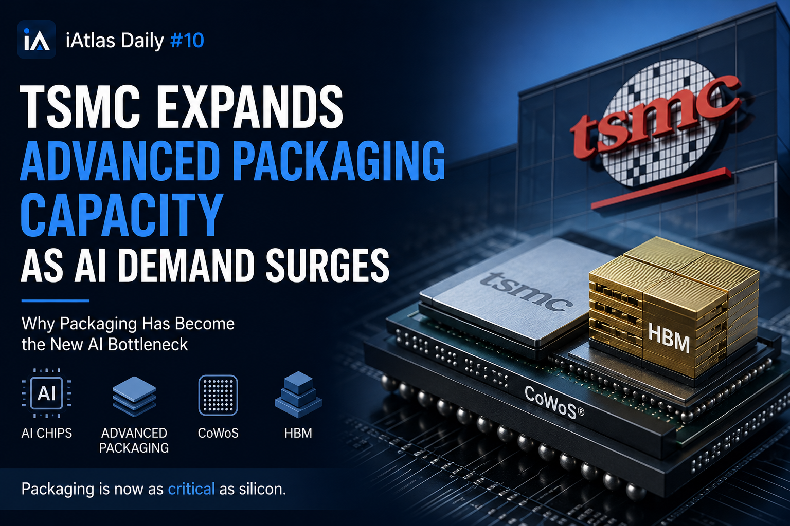
TSMC Advanced Packaging Expansion Signals the Next AI Boom | iAtlas Daily #10
Why Packaging Has Become the New AI Bottleneck
📰 iAtlas Daily #10 | July 14, 2026
📰 What Happened to TSMC Advanced Packaging?
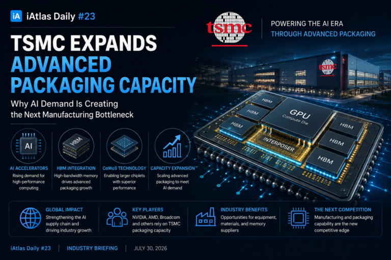
TSMC advanced packaging is expanding rapidly as AI chip demand reaches record levels.
While cutting-edge manufacturing nodes such as 3nm and 2nm often receive the most attention, industry experts increasingly identify advanced packaging as one of the biggest constraints in AI chip production.
Technologies such as CoWoS (Chip-on-Wafer-on-Substrate) are essential for integrating GPUs with High Bandwidth Memory (HBM), enabling the high-performance computing required for generative AI.
To address this growing demand, TSMC is investing aggressively in expanding its packaging facilities and production capacity.
💡 Why It Matters
TSMC advanced packaging has become one of the semiconductor industry’s most important technologies.
The AI industry is no longer limited by chip design alone.
Today’s AI processors require multiple advanced components—including GPUs, HBM, and high-speed interconnects—to be assembled into a single package.
Without advanced packaging technologies, these components cannot function as a complete AI accelerator.
As a result, packaging capacity has become just as important as semiconductor manufacturing capacity.
The competition is no longer only about making smaller chips—it’s about assembling them efficiently at scale.
🌍 Industry Impact
AI Chip Developers
Companies such as NVIDIA, AMD, and other AI accelerator developers rely heavily on TSMC’s advanced packaging technologies.
Limited packaging capacity can delay AI hardware shipments even when semiconductor fabrication is complete.
Memory Manufacturers
Growing demand for advanced packaging also benefits HBM suppliers such as SK hynix, Samsung Electronics, and Micron.
As AI chip production increases, demand for advanced memory integration continues to rise.
Semiconductor Equipment Suppliers
Expanding packaging capacity creates new opportunities for companies supplying bonding, inspection, metrology, and advanced packaging equipment.
The packaging ecosystem is rapidly becoming one of the fastest-growing segments of the semiconductor industry.
🎯 Atlas Insight
For decades, semiconductor innovation focused primarily on transistor scaling.
Today, AI is changing that equation.
Packaging has become a strategic technology rather than a manufacturing afterthought.
Companies capable of scaling advanced packaging capacity will play a critical role in determining how quickly next-generation AI infrastructure can be deployed worldwide.
📚 Related Articles
➡️ Why HBM Is Redefining AI Computing
Discover why High Bandwidth Memory has become essential for AI accelerators.
➡️ Why Glass Substrate Could Replace Today’s Chip Packaging
Learn how glass substrates could reshape the future of advanced semiconductor packaging.
About iAtlas
iAtlas is an independent publication covering batteries, semiconductors, OLED, advanced materials, AI, and global industrial trends.
We transform complex industrial developments into clear, reliable, and easy-to-understand insights.
Whether you’re following today’s industry news or building long-term expertise, iAtlas helps you understand not only what happened, but why it matters.
Technology creates change.
Insight creates opportunity.
— iAtlas