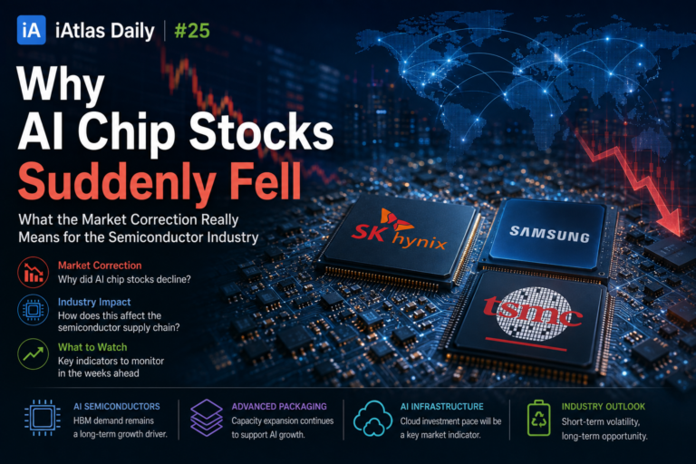
Why Glass Substrate Could Replace Today’s Chip Packaging
The Next Platform for AI Semiconductor Performance
📰 iAtlas Daily #4 | July 5, 2026
Today’s Highlights
- Glass substrates are emerging as one of the most promising innovations in advanced semiconductor packaging.
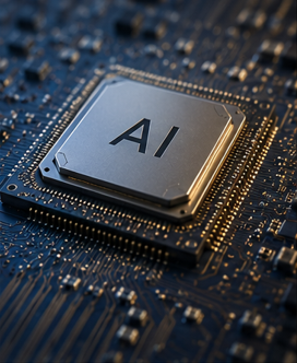
- AI processors require faster communication, lower power consumption, and improved thermal performance.
- Major chipmakers and material suppliers are accelerating investments in next-generation packaging technologies.
Cover Story
Why Chip Packaging Matters More Than Ever
For years, semiconductor innovation has focused on making transistors smaller and chips faster.
Today, however, another technology is becoming equally important:
Advanced packaging.
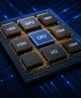
Modern AI processors no longer rely on a single chip.
Instead, multiple chiplets—including CPUs, GPUs, HBM memory, and I/O dies—are integrated into a single package.
As chip complexity increases, the substrate connecting these components becomes a critical performance factor.
This is where glass substrates are attracting growing attention.
Advanced Packaging
From Organic to Glass
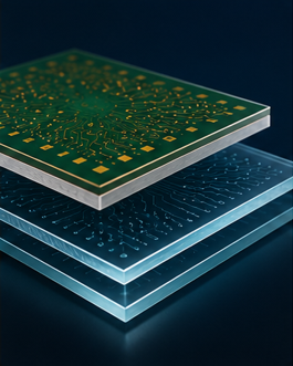
Today’s semiconductor packages primarily use organic substrates.
While these materials have supported decades of progress, future AI processors demand even greater precision.
Glass substrates offer several advantages:
- Lower thermal expansion
- Better dimensional stability
- Finer circuit patterns
- Improved electrical performance
These characteristics enable larger packages and higher interconnect density.
AI Computing
AI Needs Better Packaging
As AI models become larger, data movement inside the package becomes increasingly important.
Processors now exchange massive amounts of information with HBM memory every second.
Reducing signal loss and improving power efficiency are becoming essential.
Glass substrates could help meet these requirements while supporting future chip architectures.
Materials
Manufacturing Challenges
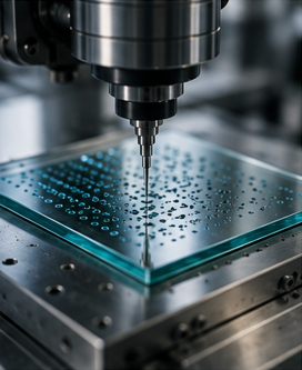
Despite their advantages, glass substrates are not easy to manufacture.
Challenges include:
- Precision drilling
- Ultra-flat surfaces
- Crack resistance
- Large-scale production
Material suppliers and equipment manufacturers are actively developing new processes to overcome these challenges.
🎯 Atlas Radar
What Is a Glass Substrate?
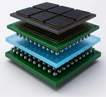
A glass substrate is a thin sheet of engineered glass used as the foundation for advanced semiconductor packaging.
Compared with conventional organic materials, glass offers superior mechanical stability and electrical performance.
Why It Matters
Future AI chips will require larger, faster, and more complex packages.
Glass substrates could become one of the enabling technologies behind next-generation AI hardware.
🔭 Atlas Outlook
Looking Ahead
Packaging Innovation Will Accelerate
Competition is shifting beyond transistor scaling toward advanced packaging technologies.
AI Demand Will Drive Adoption
As AI processors become more powerful, demand for improved package performance will continue to grow.
New Supply Chains Are Emerging
Glass manufacturers, equipment suppliers, and semiconductor companies are building new ecosystems around this technology.
💡 Atlas Insight
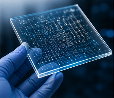
The next breakthrough in semiconductors may not come from making transistors smaller.
It may come from improving the platform that connects them.
Glass substrates represent more than a new material.
They represent a new foundation for the AI computing era.
Today’s Keywords
Glass Substrate
A next-generation substrate material designed for advanced semiconductor packaging.
Advanced Packaging
Technologies that integrate multiple semiconductor chips into a single package for higher performance.
Chiplet
A small functional semiconductor die combined with others to build a larger processor.
📚 Continue Reading
Previous Daily
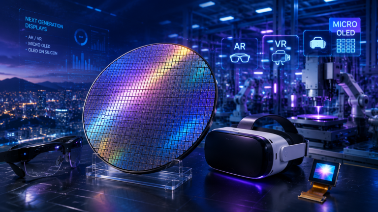
➡️ Why 300mm Wafers Matter for AR/VR
Discover how the transition to 300mm wafers is transforming Micro OLED manufacturing and enabling the next generation of AR and VR devices.
Also Recommended
➡️ Why Korea’s Chip Giants Are Investing at the Same Time
Explore how Samsung Electronics and SK hynix are preparing for the AI era through long-term investments in advanced semiconductor manufacturing.
About iAtlas
iAtlas is an independent publication covering batteries, semiconductors, OLED, advanced materials, AI, and global industrial trends.
We transform complex industrial developments into clear, reliable, and easy-to-understand insights.
Whether you’re following today’s industry news or building long-term expertise, iAtlas helps you understand not only what happened, but why it matters.
Technology creates change.
Insight creates opportunity.
— iAtlas