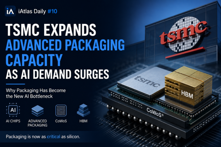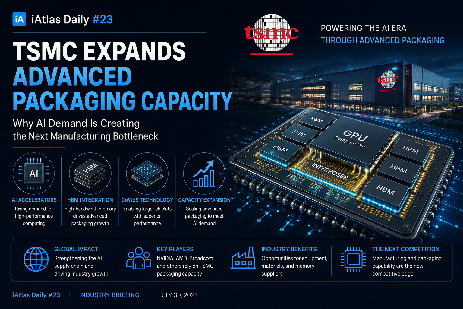
TSMC Expands Advanced Packaging Capacity
Why AI Demand Is Creating the Next Manufacturing Bottleneck
📰 iAtlas Daily #23 | July 30, 2026
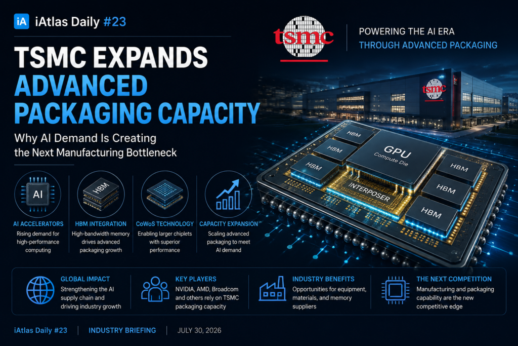
TSMC Advanced Packaging Explained
TSMC Advanced Packaging is becoming one of the most important competitive advantages in AI semiconductor manufacturing.
TSMC has continued expanding its advanced packaging facilities to support the growing demand for AI accelerators from customers including NVIDIA, AMD, and Broadcom. As AI processors become larger and integrate High-Bandwidth Memory (HBM), advanced packaging technologies such as CoWoS have become essential for delivering high-performance computing solutions.
Rather than simply manufacturing wafers, TSMC is investing heavily in packaging technologies that connect multiple chips into a single high-performance package. This shift reflects how semiconductor manufacturing is evolving beyond traditional wafer fabrication.
💡 Why This Move Matters
For many years, semiconductor performance was largely driven by transistor scaling.
Today, packaging has become equally important.
Modern AI processors combine:
- GPU
- HBM
- Interposer
- Chiplets
- High-speed interconnects
Without advanced packaging, these components cannot operate efficiently as a unified computing platform.
This explains why packaging capacity has become one of the industry’s most valuable manufacturing assets.
🌍 Industry Impact
AI Chip Designers
Companies such as NVIDIA, AMD, and Broadcom increasingly depend on advanced packaging capacity to bring new AI products to market.
Memory Suppliers
HBM manufacturers including SK hynix, Samsung Electronics, and Micron also benefit because advanced packaging directly increases HBM demand.
Semiconductor Equipment Companies
Packaging expansion creates opportunities for suppliers of:
- Flip-chip bonding equipment
- Advanced inspection systems
- Wafer bonding tools
- Thermal management technologies
Materials Industry
Demand continues to grow for:
- Advanced substrates
- Underfill materials
- Thermal interface materials
- Packaging chemicals
👀 What to Watch
Several developments will shape the next phase of AI manufacturing:
- Additional CoWoS capacity expansion
- New advanced packaging technologies
- HBM4 commercialization
- Chiplet adoption
- AI server demand through 2027
🎯 Atlas Insight
For decades, the semiconductor industry competed by building smaller transistors.
The AI era is changing that equation.
Today, the biggest competitive advantage may no longer be who designs the fastest chip—but who can manufacture and package that chip at scale.
Advanced packaging is becoming a strategic capability rather than a back-end manufacturing process.
Companies that secure packaging capacity will be better positioned to support the next generation of AI infrastructure.
📚 Related Articles
- 📘 Semiconductor Library #15 | What Is CoWoS?
- 📘 Semiconductor Library #3 | What Is HBM?
- 📰 iAtlas Daily #22 | Samsung Broadcom Partnership: How AI Manufacturing Is Changing
Sources
- TSMC Annual Report – Advanced Packaging Strategy
- TSMC Technology Overview
- TrendForce – AI Packaging Market Analysis
- Counterpoint Research – AI Semiconductor Supply Chain
- Reuters – AI Chip Demand and Advanced Packaging Developments
About iAtlas
iAtlas is an independent publication covering batteries, semiconductors, OLED, advanced materials, AI, and global industrial trends.
We transform complex industrial developments into clear, reliable, and easy-to-understand insights.
Whether you’re following today’s industry news or building long-term expertise, iAtlas helps you understand not only what happened, but why it matters.
Technology creates change.
Insight creates opportunity.
— iAtlas