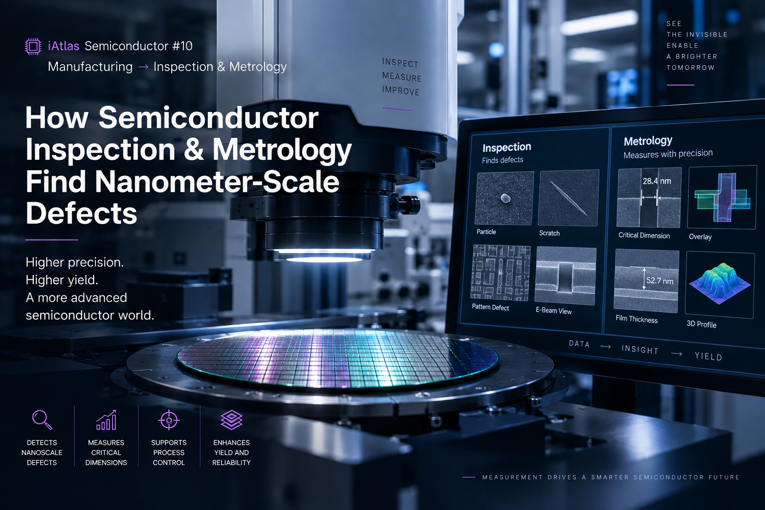
How Semiconductor Inspection & Metrology Find Nanometer-Scale Defects
💻 iAtlas Semiconductor #10 | 📘 Manufacturing → Inspection & Metrology
Introduction
Modern semiconductor manufacturing requires billions of microscopic structures to be fabricated with extraordinary precision.
A tiny particle, a pattern shifted by only a few nanometers, or a film that is slightly too thick can affect device performance or cause a chip to fail.
This is why Semiconductor Inspection and Metrology are essential throughout wafer fabrication.
Inspection searches for defects and abnormalities across the wafer, while metrology measures critical dimensions, film thickness, overlay, and other process parameters.
Together, they answer two fundamental questions:
Did the process create a defect?
and
Was the structure manufactured within specification?
As semiconductor devices become smaller and more three-dimensional, answering these questions becomes increasingly difficult—and increasingly important.
Why Semiconductor Manufacturing Needs Inspection and Metrology
Semiconductor fabrication involves hundreds or even thousands of individual process steps.
These may include:
Deposition → Photolithography → Etching → Ion Implantation → CMP → Cleaning → Inspection
Each step introduces potential variation.
For example:
- A particle may land on the wafer.
- A lithography pattern may shift.
- Etching may produce an incorrect profile.
- A deposited film may be too thick or too thin.
- CMP may remove too much material.
- A microscopic scratch may appear on the surface.
If these problems are not detected early, additional processing may continue on defective wafers.
This can increase manufacturing cost and reduce yield.
Inspection and metrology therefore act as the eyes of the semiconductor fab.
Inspection vs. Metrology
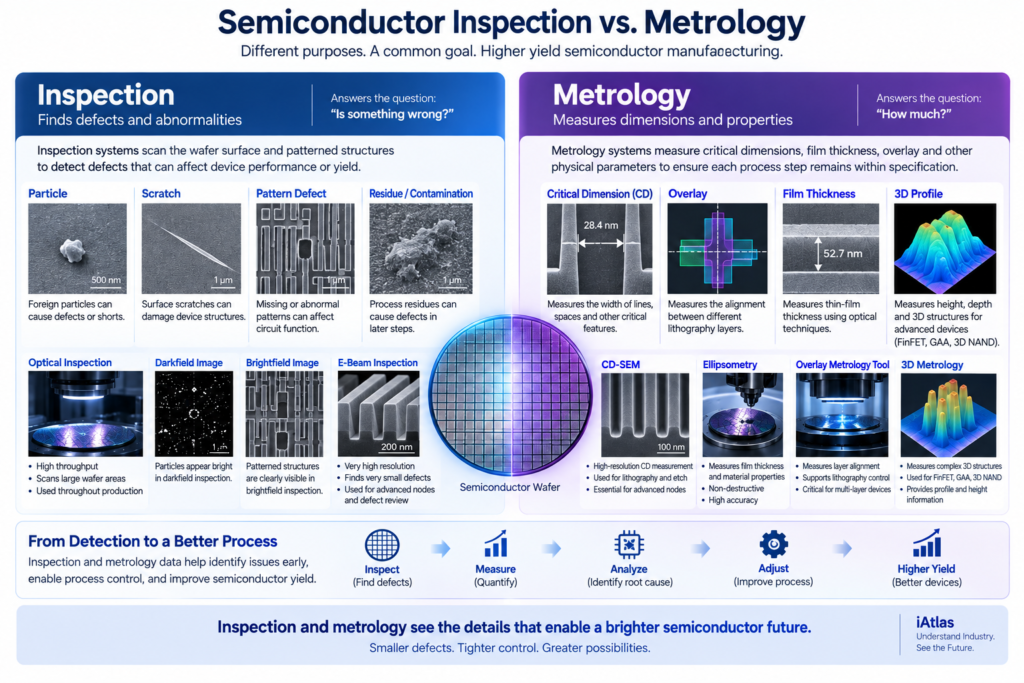
Although the terms are often discussed together, they serve different purposes.
| Inspection | Metrology |
|---|---|
| Searches for defects | Measures process parameters |
| Finds particles and abnormalities | Measures dimensions and properties |
| Answers “Is something wrong?” | Answers “How much?” |
| Often scans large wafer areas | Often measures selected structures |
| Supports defect detection | Supports process control |
Both are required.
Inspection may reveal that an abnormal feature exists, while metrology can determine whether its dimensions fall outside the allowed process window.
What Is Semiconductor Inspection?
Semiconductor inspection searches wafer surfaces and patterned structures for defects that could affect device performance or yield.
Typical defects include:
- Particles
- Scratches
- Pattern defects
- Residues
- Missing structures
- Bridging
- Voids
- Surface contamination
- Process-induced abnormalities
Inspection systems must detect extremely small defects while scanning large wafer areas at high speed.
This creates a difficult engineering challenge:
Find extremely small defects without slowing semiconductor production.
Optical Wafer Inspection
One of the most widely used inspection approaches is optical inspection.
Light is directed toward the wafer and the system analyzes reflected or scattered light.
Abnormalities can produce optical signals that differ from the surrounding structures.
Sophisticated algorithms then identify potential defects.
Optical inspection offers an important advantage:
high throughput.
Large wafer areas can be inspected relatively quickly, making optical systems suitable for monitoring production wafers throughout semiconductor manufacturing.
Brightfield and Darkfield Inspection
Optical inspection can use different illumination and detection techniques.
Brightfield Inspection
Brightfield systems analyze reflected light from the wafer.
They can provide detailed information about patterned structures and surface abnormalities.
Darkfield Inspection
Darkfield inspection emphasizes scattered light.
Particles and certain defects can scatter incoming light strongly, making them easier to detect against a darker background.
Different defect types respond differently to optical conditions, so semiconductor fabs may use multiple inspection techniques.
Why Optical Inspection Has Limits
As semiconductor structures become smaller, some defects become difficult to detect optically.
The challenge becomes particularly significant when defect dimensions approach or fall below the effective resolution of the inspection system.
This does not make optical inspection obsolete.
Instead, semiconductor manufacturing increasingly combines high-speed optical inspection with higher-resolution techniques.
Electron-Beam Inspection
Electron-beam inspection, often called e-beam inspection, uses electrons rather than visible light to examine wafer structures.
Because electrons can provide extremely high spatial resolution, e-beam systems can detect and analyze very small defects.
This makes them valuable for:
- Advanced logic
- Leading-edge memory
- Process development
- Defect review
- Nanoscale pattern analysis
However, high resolution comes with a trade-off.
E-beam inspection is generally slower than optical inspection.
Therefore, the two technologies often play complementary roles.
Optical inspection → High-speed defect discovery
E-beam inspection → High-resolution analysis
Defect Inspection and Defect Review
Finding a potential defect is only the beginning.
After an inspection system identifies suspicious locations, engineers may need to determine what actually caused the defect.
This process is called defect review.
A simplified workflow is:
Wafer Inspection
↓
Defect Coordinates Generated
↓
Defect Review
↓
Defect Classification
↓
Root Cause Analysis
↓
Process Improvement
High-resolution imaging tools such as electron microscopes can be used during defect review.
What Is Semiconductor Metrology?
While inspection searches for defects, semiconductor metrology measures the physical characteristics of semiconductor structures.
Important measurements include:
- Critical Dimension (CD)
- Overlay
- Film thickness
- Wafer shape
- Surface topography
- Material properties
- Pattern profile
- Step height
These measurements allow engineers to determine whether each manufacturing process remains within specification.
Critical Dimension Metrology
One of the most important measurements in semiconductor manufacturing is the Critical Dimension (CD).
CD refers to the dimensions of important patterned features.
For example, semiconductor engineers may need to measure the width of:
- Lines
- Spaces
- Gates
- Trenches
- Contacts
- Other nanoscale structures
As device dimensions shrink, even small CD variations can affect electrical performance.
CD-SEM
A widely used tool for measuring semiconductor pattern dimensions is the Critical Dimension Scanning Electron Microscope (CD-SEM).
A CD-SEM scans an electron beam across semiconductor structures and uses the resulting signals to determine their dimensions.
Compared with conventional optical measurement, electron microscopy can provide much higher resolution.
CD-SEM measurements are widely used to monitor lithography and etching processes.
For example:
Photolithography
↓
CD Measurement
↓
Etching
↓
CD Measurement
Comparing measurements before and after etching helps engineers understand how the process changes the pattern.
What Is Overlay Metrology?
Modern chips contain many patterned layers stacked on top of one another.
Each new lithography layer must align precisely with structures already formed on the wafer.
The positional difference between layers is called overlay error.
Overlay metrology measures this alignment.
If overlay error becomes too large, structures from different layers may not connect correctly.
This can cause:
- Electrical failure
- Short circuits
- Open circuits
- Reduced device performance
- Yield loss
Overlay control becomes increasingly challenging as semiconductor dimensions shrink.
Why Overlay Is So Difficult
A wafer is not perfectly rigid or geometrically stable throughout fabrication.
Processes can introduce:
- Thermal expansion
- Film stress
- Wafer distortion
- Pattern deformation
- Local process variation
Therefore, overlay control requires more than simply aligning two images.
Advanced metrology systems analyze complex wafer-level and local variations to help lithography systems compensate for these effects.
Film Thickness Metrology
Deposition processes such as CVD, PVD, and ALD create thin material layers on semiconductor wafers.
These layers must often be controlled at nanometer-scale thicknesses.
Film thickness metrology can use optical techniques such as:
- Reflectometry
- Ellipsometry
- Spectroscopic measurement
By analyzing how light interacts with the film, these systems can estimate properties such as thickness and optical characteristics.
Why Film Thickness Matters
Incorrect film thickness can influence:
- Electrical resistance
- Capacitance
- Device isolation
- Etching behavior
- Pattern formation
- Mechanical stress
For this reason, deposition and CMP processes frequently depend on metrology feedback.
The manufacturing loop can look like:
Process → Measure → Analyze → Adjust → Process
This feedback loop is fundamental to advanced process control.
3D Metrology
Traditional semiconductor devices could often be characterized primarily using two-dimensional measurements.
Modern devices are different.
Technologies such as:
- FinFET
- Gate-All-Around (GAA)
- 3D NAND
- TSV
- Advanced packaging
contain complex three-dimensional structures.
Engineers increasingly need to understand not only width and length but also:
- Height
- Depth
- Sidewall angle
- Profile
- Layer shape
- Buried structures
This has increased demand for advanced 3D metrology.
Measuring High-Aspect-Ratio Structures
3D NAND provides a good example.
Modern NAND devices contain deep, narrow structures created through many stacked layers.
These structures can have extremely high aspect ratios.
Engineers need to monitor characteristics such as:
- Hole depth
- Sidewall profile
- Critical dimension
- Etch uniformity
- Layer alignment
Traditional surface-only measurements may not provide enough information.
This is driving new inspection and metrology technologies.
Why Defect Size Is Not the Only Factor
A small defect is not automatically harmless.
Its impact depends on where it occurs.
A tiny defect in a non-critical region may have little effect.
The same defect located inside an important transistor or interconnect structure could cause device failure.
Therefore, modern inspection increasingly considers:
Defect size + Defect location + Device design
This makes defect analysis more intelligent than simply counting particles.
Defect Classification
Inspection tools can generate enormous numbers of defect candidates.
Engineers cannot manually analyze every image.
Automated classification systems therefore group defects according to characteristics such as:
- Shape
- Size
- Location
- Pattern
- Signal characteristics
This helps engineers identify recurring defect signatures and trace them back to specific manufacturing processes.
AI and Machine Learning in Inspection
The amount of inspection data generated by modern fabs continues to grow.
AI and machine learning are increasingly used to analyze this information.
Potential applications include:
- Automatic defect classification
- Pattern recognition
- Defect clustering
- Root-cause identification
- Process drift detection
- Predictive yield analysis
Instead of simply detecting defects, future inspection systems increasingly aim to explain why defects are occurring.
Inspection, Metrology, and Yield
Semiconductor yield represents the percentage of manufactured dies that meet required specifications.
Inspection and metrology directly support yield improvement.
Consider a simplified example.
A deposition process begins producing slightly thicker films than expected.
Metrology detects the shift before it causes widespread failures.
Engineers adjust the process.
Production returns to the target range.
Without measurement, the problem might remain unnoticed until electrical testing much later in manufacturing.
Early detection can therefore save significant time and manufacturing cost.
Process Control Through Data
Inspection and metrology create enormous amounts of manufacturing data.
This data can be connected with process equipment information from:
- Lithography systems
- Etchers
- Deposition equipment
- Ion implanters
- CMP systems
Combining these datasets allows fabs to understand relationships between equipment conditions and wafer results.
This is one of the foundations of Advanced Process Control (APC).
Sampling vs. Full-Wafer Inspection
Not every measurement can be performed on every location of every wafer.
High-resolution measurements can require significant time.
Manufacturers therefore develop sampling strategies.
They must decide:
- Which wafers should be measured?
- Which wafer locations are most important?
- How frequently should measurements occur?
- Which process steps require more inspection?
The objective is to collect enough information for reliable process control without creating excessive manufacturing delays.
The Throughput vs. Resolution Challenge
Inspection technology constantly faces a fundamental trade-off.
Higher resolution
Can detect smaller defects but may require more measurement time.
Higher throughput
Can scan more wafers but may provide less detailed information.
Modern semiconductor fabs therefore use multiple technologies together.
For example:
Fast Optical Inspection
↓
Identify Suspicious Locations
↓
High-Resolution E-Beam Review
↓
Classify Defect
↓
Identify Root Cause
This combination provides both production speed and detailed analysis.
Inspection & Metrology Equipment
Inspection and metrology systems can include:
- Optical wafer inspection
- E-beam inspection
- Defect review SEM
- CD-SEM
- Overlay metrology
- Film thickness metrology
- Optical critical dimension measurement
- Surface profiling
- X-ray-based measurement
- Advanced 3D metrology
Companies such as KLA, Applied Materials, Hitachi High-Tech, and Onto Innovation develop technologies used across different parts of this field.
Why Inspection & Metrology Are Becoming More Important
Semiconductor scaling makes manufacturing tolerances increasingly narrow.
At the same time, device architectures are becoming more complex.
The industry is moving toward:
- Gate-All-Around transistors
- High-NA EUV
- High-layer-count 3D NAND
- HBM
- Chiplets
- Hybrid bonding
- Advanced 3D packaging
These technologies introduce new structures, interfaces, and potential defect mechanisms.
Inspection and metrology must evolve alongside them.
The Future of Semiconductor Inspection
Future inspection systems will need to detect smaller defects across increasingly complex structures while maintaining production throughput.
Key development areas include:
- Higher-resolution optical inspection
- Faster e-beam inspection
- Advanced 3D metrology
- AI-based defect classification
- Computational metrology
- Hybrid measurement techniques
- Improved buried-defect detection
- Equipment-to-metrology data integration
- Real-time process control
The long-term direction is clear:
Measure more → understand faster → correct earlier.
Key Takeaways
- Semiconductor Inspection identifies defects and abnormalities on wafers.
- Semiconductor Metrology measures dimensions, alignment, thickness, and other process parameters.
- Optical inspection provides high throughput, while e-beam technologies provide higher resolution.
- CD-SEM measures critical semiconductor pattern dimensions.
- Overlay metrology determines how accurately different lithography layers are aligned.
- Film metrology monitors thin-film thickness and material characteristics.
- Advanced 3D devices require increasingly sophisticated measurement technologies.
- Inspection and metrology data are essential for process control and yield improvement.
- AI is becoming increasingly important for defect classification and manufacturing-data analysis.
Frequently Asked Questions
What is semiconductor inspection?
Semiconductor inspection searches wafers for particles, scratches, pattern defects, residues, and other abnormalities that may affect device performance or yield.
What is semiconductor metrology?
Semiconductor metrology measures physical parameters such as critical dimensions, overlay, film thickness, and surface characteristics to determine whether semiconductor processes remain within specification.
What is the difference between inspection and metrology?
Inspection primarily identifies whether defects or abnormalities exist. Metrology quantitatively measures dimensions and material properties.
What is a CD-SEM?
A Critical Dimension Scanning Electron Microscope uses an electron beam to measure the dimensions of nanoscale semiconductor patterns.
Why is overlay metrology important?
Semiconductor devices contain many patterned layers. Overlay metrology determines whether these layers are correctly aligned with one another.
Why are both optical and e-beam inspection used?
Optical inspection provides the throughput needed to scan large wafer areas, while e-beam techniques provide higher resolution for analyzing very small defects and structures.
📖 Semiconductor Learning Path
Previous: 💻 Semiconductor #9 | How CMP Creates an Ultra-Flat Semiconductor Surface
⬇️
Current: 💻 Semiconductor #10 | How Semiconductor Inspection & Metrology Find Nanometer-Scale Defects
⬇️
Next: 💻 Semiconductor #11 | How Thermal Oxidation Grows Silicon Dioxide on a Wafer
📚 Continue Reading
- 💻 Semiconductor #5 | How Photolithography Creates Billions of Transistors
- 💻 Semiconductor #6 | How Plasma Etching Shapes Semiconductor Devices
- 💻 Semiconductor #7 | How Thin Film Deposition Builds Semiconductor Devices Layer by Layer
- 💻 Semiconductor #9 | How CMP Creates an Ultra-Flat Semiconductor Surface
- 💻 Semiconductor #11 | How Thermal Oxidation Grows Silicon Dioxide on a Wafer
References
- KLA — Semiconductor Process Control, Inspection & Metrology
- Applied Materials — E-Beam Inspection and Metrology
- Hitachi High-Tech — CD-SEM / Semiconductor Metrology
- Onto Innovation — Optical Metrology and Inspection
- SEMI — Semiconductor Manufacturing and Process Control
🔷 About iAtlas
iAtlas is an independent publication covering batteries, semiconductors, OLED, advanced materials, AI, and global industrial trends.
We transform complex industrial developments into clear, reliable, and easy-to-understand insights.
Whether you’re following today’s industry news or building long-term expertise, iAtlas helps you understand not only what happened, but why it matters.
Technology creates change.
Insight creates opportunity.
— iAtlas