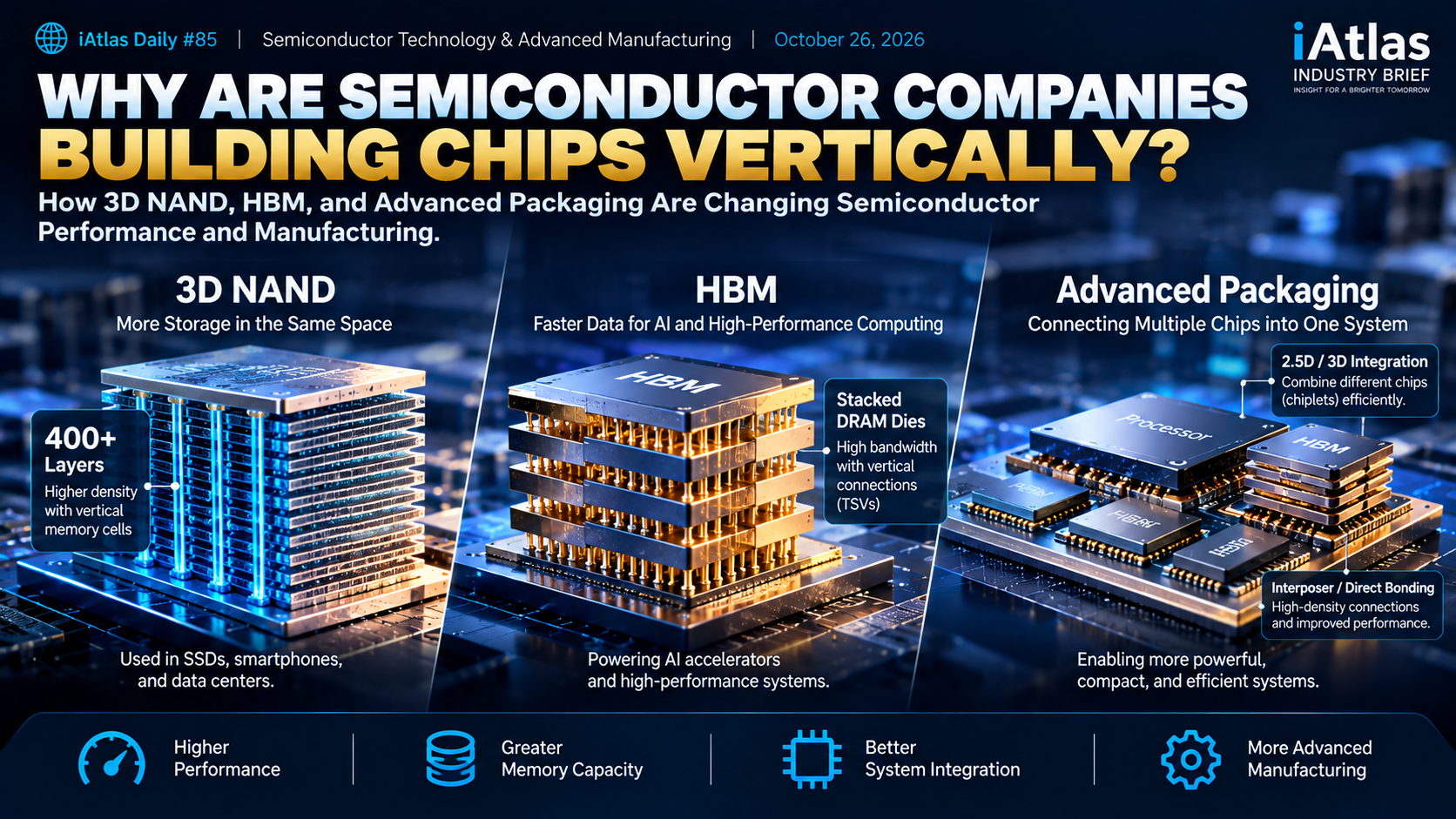
Why Are Semiconductor Companies Building Chips Vertically?
How 3D NAND, HBM, and Advanced Packaging Are Changing Semiconductor Performance and Manufacturing
iAtlas Daily #85 | Semiconductor Technology & Advanced Manufacturing | October 26, 2026
The Future of Semiconductors Is No Longer Just About Making Chips Smaller
3D semiconductor technology is changing how the industry improves performance, increases memory capacity, and designs the next generation of computing systems.
For decades, semiconductor progress was largely associated with one idea: making transistors smaller.
Smaller transistors allowed engineers to place more components on a chip, helping computers become faster, more powerful, and more energy-efficient.
But as semiconductor manufacturing approaches increasingly difficult physical and economic limits, companies are exploring another direction.
Instead of expanding only across the surface of a chip, they are building upward.
Memory cells can be arranged in hundreds of vertical layers. Multiple memory dies can be stacked into compact packages. Different chips can be connected through advanced integration technologies.
This shift is already transforming semiconductor manufacturing.
Samsung Electronics, SK Hynix, TSMC, and other semiconductor companies are investing in different forms of three-dimensional integration.
Although these technologies serve different purposes, they share a common goal:
Achieving greater computing capability without depending exclusively on smaller transistors.
1. Why Traditional Semiconductor Scaling Is Becoming More Difficult
Modern semiconductor manufacturing has benefited enormously from transistor miniaturization.
By reducing the dimensions of electronic components, manufacturers have increased transistor density and improved performance over multiple generations.
However, continued scaling is becoming more challenging.
As structures shrink, manufacturers must address several problems.
Physical Limitations
Extremely small semiconductor structures are increasingly affected by leakage currents, electrical interference, and variations in material properties.
These effects can make reliable device operation more difficult.
Manufacturing Complexity
Advanced semiconductor production requires increasingly sophisticated lithography, deposition, etching, inspection, and process-control technologies.
Smaller structures demand tighter tolerances and more complex manufacturing sequences.
Rising Costs
Advanced manufacturing equipment and process development require substantial investment.
Even when further miniaturization is technically possible, it may not always offer the most economical path to better system performance.
This does not mean transistor scaling has stopped.
Leading semiconductor manufacturers continue to develop smaller process nodes and new transistor architectures.
However, vertical integration is becoming an increasingly important complementary strategy.
2. 3D NAND: Building Memory Cells Upward
One of the clearest examples of vertical semiconductor development is 3D NAND flash memory.
NAND flash is used in solid-state drives, smartphones, computers, and data-center storage systems.
Traditional planar NAND arranged memory cells primarily across the surface of a silicon wafer.
As manufacturers attempted to increase storage density, shrinking the distance between cells created growing technical challenges.
3D NAND changed the architecture.
Instead of placing all memory cells in a single plane, manufacturers began stacking them vertically.
This allows more data to be stored within a similar chip footprint.
Samsung’s 400-Layer Milestone
At Future of Memory and Storage 2026 in August, Samsung Electronics unveiled its V10 BV-NAND technology featuring more than 400 vertically stacked layers.
According to Samsung, the new architecture improves memory density by approximately 58% compared with its previous V9 generation.
The company also introduced wafer-bonding technology and a three-stack manufacturing approach to support its increasingly complex NAND architecture.
These innovations illustrate how semiconductor manufacturers are combining structural design with advanced manufacturing techniques.
But increasing the number of layers is not simply a matter of repeating the same process.
As memory structures become taller, manufacturers face difficult challenges involving deep etching, thin-film uniformity, structural alignment, and defect control.
The greater the number of layers, the more important manufacturing precision becomes.
3. HBM: Stacking Memory to Move Data Faster
Another important example is High Bandwidth Memory, commonly known as HBM.
HBM is particularly important for AI accelerators and high-performance computing systems.
Modern AI processors perform enormous numbers of calculations.
However, processing power alone is not enough.
These systems must continuously move large amounts of data between memory and computing components.
If memory cannot deliver data quickly enough, even a powerful processor may spend time waiting.
HBM helps address this problem.
How HBM Works
Instead of relying on a conventional arrangement of separate memory chips, HBM stacks multiple DRAM dies vertically.
The dies are interconnected using technologies such as Through-Silicon Vias, or TSVs.
These vertical electrical connections allow data to move between stacked memory layers.
HBM also uses a wide memory interface to support high data-transfer bandwidth.
The result is a compact memory architecture designed for demanding computing applications.
Why AI Is Accelerating HBM Development
AI training and inference require increasingly large memory capacity and bandwidth.
This makes advanced memory integration strategically important.
Samsung and SK Hynix are developing successive generations of HBM technology to meet these requirements.
However, HBM manufacturing presents substantial challenges.
Stacked dies must be accurately aligned, bonded, electrically connected, and thermally managed.
Heat removal becomes especially important as more memory dies are integrated into compact structures.
HBM therefore represents more than a memory-design innovation.
It is also an advanced manufacturing and packaging challenge.
4. Advanced Packaging: Connecting Different Chips into One System
Vertical semiconductor integration extends beyond memory.
Increasingly, semiconductor companies are combining multiple specialized chips within a single package.
This approach is often described as heterogeneous integration.
Rather than manufacturing every function on one large silicon die, designers can divide a system into smaller components called chiplets.
Different chiplets may use different manufacturing processes, materials, or architectures.
Advanced packaging technologies then connect these components to function as a larger system.
TSMC’s 3DFabric Strategy
TSMC has developed several technologies under its 3DFabric platform.
These include CoWoS and SoIC.
CoWoS enables advanced integration of processors and memory using interposer-based packaging approaches.
It is particularly important for high-performance computing systems that combine AI processors with HBM stacks.
SoIC focuses on high-density three-dimensional chip integration.
By connecting semiconductor dies through fine-pitch bonding technologies, SoIC can reduce interconnection distances and improve integration density.
TSMC reports that its 3nm SoIC stacking technology entered volume production in 2025.
These developments demonstrate how advanced packaging is becoming an important part of semiconductor innovation.
Importantly, not every advanced packaging method stacks all chips directly on top of one another.
Some technologies, including CoWoS, primarily use 2.5D integration, placing multiple components side by side on an interposer.
Others, such as SoIC, enable direct three-dimensional stacking.
The distinction matters because each architecture involves different manufacturing processes and performance trade-offs.
5. Three Technologies, Three Different Objectives
Although 3D NAND, HBM, and advanced packaging all use vertical structures or advanced integration, they are not interchangeable technologies.
| Technology | Main Objective | Core Approach |
|---|---|---|
| 3D NAND | Increase data storage density | Stack memory cells vertically within a memory structure |
| HBM | Increase memory bandwidth | Stack DRAM dies with high-density vertical connections |
| Advanced Packaging | Improve system-level integration | Connect multiple semiconductor dies or chiplets using 2.5D and 3D technologies |
This distinction explains why semiconductor companies are pursuing multiple integration strategies simultaneously.
3D NAND addresses storage density.
HBM addresses high-speed data access.
Advanced packaging addresses the challenge of combining computing, memory, and specialized functions efficiently.
Together, they represent a broader shift toward system-level semiconductor optimization.
6. Why Vertical Integration Makes Manufacturing More Difficult
Building semiconductor structures vertically creates new opportunities, but also introduces significant production challenges.
High-Aspect-Ratio Etching
In advanced 3D NAND manufacturing, extremely deep and narrow structures must be etched through many material layers.
Maintaining consistent dimensions throughout these structures is difficult.
Small deviations can affect device performance and production yield.
Thin-Film Deposition
Complex semiconductor structures require precise deposition of insulating, conductive, and functional materials.
As structures become taller and more intricate, achieving uniform film thickness and material properties becomes increasingly challenging.
Bonding and Alignment
Stacked semiconductor dies must be accurately aligned and connected.
Advanced bonding processes require extremely clean surfaces and precise dimensional control.
Even microscopic defects can affect electrical connections and device reliability.
Thermal Management
Vertically integrated semiconductor devices can concentrate heat within a smaller physical volume.
Designers must consider how heat moves through stacked structures and how it can be removed efficiently.
Inspection and Quality Control
Defects inside complex three-dimensional structures can be difficult to detect.
Manufacturers therefore need increasingly sophisticated metrology, inspection, and process-control technologies.
These challenges explain why vertical integration is not simply a design trend.
It is driving innovation throughout the semiconductor manufacturing equipment industry.
7. Industry Implications: A New Competitive Landscape
The transition toward three-dimensional semiconductor architectures could reshape competition across the industry.
Memory Manufacturers
Samsung Electronics, SK Hynix, and other memory companies must develop increasingly sophisticated stacking, bonding, and manufacturing capabilities.
Competition will depend not only on memory specifications but also on yield, cost, reliability, and production capacity.
Semiconductor Foundries
Foundries such as TSMC are expanding their role beyond traditional wafer fabrication.
Advanced packaging and heterogeneous integration are becoming important elements of their technology portfolios.
Manufacturing Equipment Suppliers
Equipment used for deposition, etching, bonding, inspection, and metrology is becoming increasingly important.
More complex device architectures can create demand for advanced process technologies and tighter manufacturing control.
Materials Suppliers
Three-dimensional semiconductor structures require high-performance dielectric materials, conductors, bonding materials, and specialized process chemicals.
Material purity, consistency, and compatibility become critical as manufacturing tolerances tighten.
AI and Data-Center Infrastructure
The integration of processors and high-bandwidth memory is becoming central to AI system performance.
Future computing advances may increasingly depend on improvements in data movement, memory integration, and energy efficiency rather than processor performance alone.
iAtlas Insight | The Next Semiconductor Advantage May Come from Integration
For decades, semiconductor competition was often summarized by a simple question:
Who can manufacture the smallest transistors?
That question remains important.
But it is no longer sufficient.
A semiconductor company may develop an advanced manufacturing node and still face limitations involving memory bandwidth, data movement, packaging, or thermal management.
This is why vertical integration is becoming strategically significant.
Three factors will shape the next phase of competition.
1. Architecture
Companies must determine how to combine computing, memory, and storage functions efficiently.
2. Manufacturing Capability
Advanced structures require precise etching, deposition, bonding, and inspection processes.
3. System-Level Economics
Performance improvements must justify manufacturing complexity, production costs, and reliability requirements.
The most competitive semiconductor companies may therefore be those capable of optimizing the entire system rather than focusing exclusively on individual components.
For equipment and materials suppliers, this transition could create opportunities in advanced deposition, high-aspect-ratio etching, wafer bonding, surface preparation, and process monitoring.
For the broader technology industry, it suggests a fundamental shift.
The future of semiconductor performance will depend not only on how small chips become, but also on how intelligently they are built and connected.
Related Articles
Semiconductor Manufacturing
How Thin Film Deposition Builds Semiconductor Devices Layer by Layer
Explore how precision thin-film deposition supports increasingly complex semiconductor structures and advanced manufacturing processes.
Industrial Supply Chains
Industrial Competition Is Moving Deeper into the Supply Chain
Understand why semiconductor equipment, materials, and upstream manufacturing capabilities are becoming important sources of industrial competitiveness.
Manufacturing Strategy
The Next Industrial Advantage Is Flexibility
Discover why manufacturing adaptability is becoming increasingly valuable as technology and production requirements evolve.
References
1. Samsung Electronics — Samsung Unveils Next-Gen 3D-Memory Vision at FMS 2026 (August 2026)
Official announcement of Samsung’s V10 BV-NAND with more than 400 layers, next-generation 3D memory architectures, and wafer-bonding innovations.
2. Samsung Semiconductor — 3D V-NAND Flash Memory
Technical explanation of vertical NAND memory architecture and its development beyond planar memory structures.
3. TSMC — HPC Platform and 3DFabric Technologies
Official technical overview of CoWoS, heterogeneous integration, advanced packaging, and high-performance computing applications.
4. TSMC — System on Integrated Chips (SoIC)
Official description of TSMC’s three-dimensional chip-stacking technology, high-density interconnections, and advanced integration capabilities.
Corporate reporting on advanced semiconductor manufacturing, 3DFabric, SoIC, and the growing role of advanced packaging.
ℹ️ About iAtlas
iAtlas is an independent publication covering batteries, semiconductors, OLED, advanced materials, AI, and global industrial trends.
We transform complex industrial developments into clear, reliable, and easy-to-understand insights.
Whether you’re following today’s industry news or building long-term expertise, iAtlas helps you understand not only what happened, but why it matters.
Technology creates change.
Insight creates opportunity.
— iAtlas