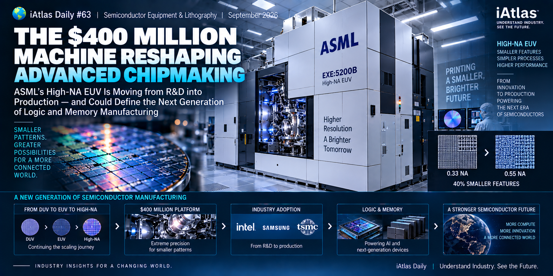
The $400 Million Machine Reshaping Advanced Chipmaking
ASML’s High-NA EUV Is Moving from R&D into Production — and Could Define the Next Generation of Logic and Memory Manufacturing
⚙️ iAtlas Daily #63 | Semiconductor Equipment & Lithography | September 2026
Some of the world’s most advanced semiconductor factories are preparing for a new generation of manufacturing equipment.
The machine costs roughly:
$400 Million
It uses extreme ultraviolet light.
Its optics are among the most sophisticated ever manufactured.
And its purpose is surprisingly simple:
Print smaller patterns on silicon.
The machine is ASML’s:
High-NA EUV Lithography System
High-NA increases the numerical aperture of EUV lithography from:
0.33
to:
0.55
allowing chipmakers to print significantly smaller features than today’s conventional EUV systems. ASML says its EXE High-NA platform can achieve 8 nm resolution using 13.5 nm EUV light.
The technology is now moving beyond experimentation.
Intel has already used High-NA EUV on selected layers of commercial processors.
Samsung plans to introduce it into future DRAM high-volume manufacturing.
TSMC intends to deploy it for advanced-node production.
High-NA is therefore entering a critical transition:
Technology Development
↓
Process Qualification
↓
Production
↓
Industry Adoption
And that makes a $400 million machine strategically important to the future of semiconductor manufacturing.
🌍 The Big Story
Semiconductor manufacturing depends on one fundamental capability:
Patterning
A chip contains billions of microscopic structures.
To manufacture them, chipmakers repeatedly transfer circuit patterns onto silicon wafers.
The smaller those patterns become, the more transistors engineers can potentially fit into a given area.
That enables improvements in:
Performance
Power Efficiency
Density
and:
Computing Capability
For decades, lithography technology has been one of the key technologies enabling this progression.
The evolution has broadly moved through:
DUV
↓
Immersion DUV
↓
EUV
↓
High-NA EUV
The latest transition is now beginning.
🔬 1. What Does a Lithography Machine Actually Do?
Think of semiconductor lithography as an extraordinarily sophisticated printing process.
A simplified flow looks like:
Circuit Pattern
↓
Photomask
↓
Light
↓
Optical System
↓
Photoresist-Coated Wafer
↓
Pattern Transfer
The machine projects a microscopic circuit pattern onto the wafer.
But modern semiconductor features are incredibly small.
That means the lithography system must control:
Light
Optics
Wafer Position
Focus
Alignment
and:
Vibration
with extreme precision.
Small errors can affect the chip pattern.
And pattern errors can affect yield.
💡 2. Why Did the Industry Need EUV?
Earlier semiconductor manufacturing relied heavily on deep ultraviolet lithography.
But as semiconductor features became smaller, manufacturers needed increasingly complex techniques to continue scaling.
One solution was:
Multiple Patterning
Instead of creating a feature with one exposure, manufacturers divide the pattern across several process steps.
Conceptually:
One Complex Pattern
↓
Exposure 1
Exposure 2
Exposure 3
Additional Processing
This works.
But complexity increases.
More process steps can mean:
More Equipment
More Time
More Cost
More Opportunities for Defects
EUV helped simplify some of those critical layers.
Now High-NA attempts to extend that advantage further.
🔭 3. What Does “High NA” Actually Mean?
NA stands for:
Numerical Aperture
Without going too deeply into optical physics, numerical aperture influences how finely a lithography system can resolve patterns.
Today’s standard EUV systems use:
NA = 0.33
High-NA EUV increases that to:
NA = 0.55
Higher numerical aperture enables finer resolution.
ASML’s EXE systems use the same 13.5 nm EUV wavelength, but redesigned optics enable higher contrast and approximately 8 nm resolution.
So the transition is:
Low-NA EUV
0.33 NA
↓
High-NA EUV
0.55 NA
↓
Smaller Printable Features
That sounds like a relatively small numerical change.
Technically, it is enormous.
📏 4. High-NA Can Print About 40% Smaller Features
According to recent reporting, High-NA systems can print features approximately 40% smaller than conventional EUV equipment.
This matters because advanced chips increasingly depend on extremely dense structures.
For logic:
Smaller Transistors
→ More density
→ Higher performance potential
For memory:
Smaller Memory Cells
→ More capacity per area
→ Improved manufacturing economics
This makes High-NA relevant to both:
Logic
and:
Memory
That is why companies with very different semiconductor businesses are evaluating the same machine.
💰 5. Why Does One Machine Cost Around $400 Million?
High-NA EUV is not simply a slightly improved EUV scanner.
The system required major changes in:
Optics
Stages
Metrology
Masks
Resists
Computational Lithography
and:
Fab Infrastructure
The machine itself is extraordinarily complex.
Reuters estimates High-NA tools cost roughly $400 million each.
That creates an extraordinary economic question.
Why would a semiconductor manufacturer spend hundreds of millions of dollars on one lithography system?
Because the relevant calculation is not:
How much does the machine cost?
It is:
How much does the process cost without it?
🧩 6. Process Simplification Is the Real Economic Argument
This is one of the most important points in understanding High-NA.
A more capable lithography system may eliminate multiple manufacturing steps.
ASML reported earlier this year that customer work showed cases in both logic and DRAM where:
1 High-NA exposure
could replace:
3–4 Low-NA exposures
for certain applications.
For some critical layers, ASML says High-NA could reduce the total number of process steps by as much as a factor of ten.
So the economics can look like:
More Expensive Scanner
but potentially:
Fewer Exposures
Fewer Process Steps
Shorter Cycle Time
Lower Defect Opportunities
This is why equipment price alone does not determine manufacturing economics.
🏭 7. Intel Has Already Crossed an Important Line
High-NA is no longer confined entirely to R&D.
Intel Foundry is using High-NA EUV on selected layers of its Intel 18A process for a subset of Core Ultra Series 3 processors.
ASML announced in July that these products had entered high-volume manufacturing and were shipping to customers.
Intel and ASML subsequently reported that more than:
1 Million Wafers
had been processed using High-NA systems across certification, R&D and production activities.
Intel says throughput, overlay and availability are meeting its expectations.
This is a major milestone.
The question used to be:
Can High-NA work?
Now the industry can increasingly ask:
Where does using High-NA make economic sense?
🇰🇷 8. Samsung Is Taking High-NA into DRAM
High-NA is not only a logic technology.
Samsung Electronics announced this month that it plans to introduce ASML High-NA EUV into:
Future DRAM High-Volume Manufacturing
by 2028.
ASML and Samsung describe this as the industry’s first planned High-NA deployment for DRAM mass production.
This is especially important for Korea.
Samsung already uses EUV extensively in advanced semiconductor manufacturing.
High-NA could help extend DRAM scaling by enabling:
Improved Resolution
↓
Simpler Patterning
↓
Fewer Complex Multi-Patterning Steps
↓
Potential Manufacturing Efficiency
Memory therefore represents another major market for ASML’s next-generation lithography platform.
🇰🇷 9. SK hynix Is Also Part of the High-NA Transition
SK hynix is another important potential adopter.
The company has been evaluating High-NA for advanced memory manufacturing, while industry adoption among leading memory producers is expected to accelerate around the 2027–2028 period. ASML has said its High-NA platform is being matured with customers toward broader high-volume-manufacturing insertion.
This is strategically important because advanced memory scaling is becoming increasingly difficult.
Future:
DRAM
HBM Base Dies
and other advanced memory structures may require more sophisticated patterning.
Lithography therefore remains a core part of memory competition.
🇹🇼 10. TSMC Is Taking a More Gradual Approach
TSMC’s timetable is different.
The company intends to introduce High-NA EUV into high-volume manufacturing for advanced nodes starting around:
2030
As nodes advance, TSMC expects more layers to require High-NA, particularly as transistor structures become increasingly complex.
This highlights an important feature of semiconductor manufacturing.
There is rarely one universal adoption schedule.
Different manufacturers evaluate:
Cost
Process Complexity
Yield
Product Architecture
and:
Technology Roadmaps
differently.
Intel moved early.
Samsung is targeting DRAM in 2028.
TSMC plans broader advanced-node adoption around 2030.
High-NA adoption will therefore occur gradually.
🎭 11. There Is Still a Mask Problem
High-NA introduces another challenge.
The optical architecture changes the size of the printable field.
This can create limitations for very large chips.
That matters because some of today’s most important AI processors are enormous.
Think about:
GPU
AI Accelerator
Data-Center Processor
These chips push reticle-size limits.
One potential solution is:
Larger Photomasks
ASML and TSMC recently launched an industry initiative to develop 12-inch photomasks for High-NA EUV.
Samsung and other ecosystem participants are also joining the effort.
📐 12. Why Move from 6-Inch to 12-Inch Masks?
The semiconductor industry has used the current mask format for decades.
High-NA changes the economics.
Larger masks could help:
Increase Scanner Productivity
Reduce Stitching Constraints
Support Larger Chips
and:
Lower Manufacturing Costs
The current roadmap targets:
12-inch Mask Pilot Line
→ 2031
and:
Advanced Production Readiness
→ 2033.
This illustrates something important.
A lithography revolution requires much more than a lithography machine.
🔗 13. High-NA Requires an Entire Ecosystem
To make High-NA commercially successful, the industry needs:
Scanner
↓
Optics
↓
Light Source
↓
Photomask
↓
Photoresist
↓
Metrology
↓
EDA
↓
Process Integration
↓
Fab
Every layer needs to work.
This is exactly why semiconductor manufacturing is so difficult.
A breakthrough at one layer can require simultaneous innovation across many others.
🧪 14. Photoresist Is Also Critical
Lithography does not print directly onto bare silicon.
The wafer is coated with a light-sensitive material:
Photoresist
When EUV light hits the resist, chemical reactions allow the pattern to be transferred.
As features shrink, resist performance becomes increasingly important.
The material must balance:
Resolution
Sensitivity
Roughness
Defectivity
High-NA therefore creates opportunities not only for ASML.
It creates requirements across the semiconductor materials industry.
Again:
Equipment innovation
creates:
Materials innovation
🔍 15. Metrology Becomes Harder Too
You cannot manufacture what you cannot measure.
As patterns become smaller, semiconductor manufacturers need increasingly sophisticated inspection and metrology.
They must measure:
Critical Dimensions
Overlay
Defects
Pattern Placement
Film Thickness
High-NA therefore also increases demand for technologies surrounding the lithography process.
The machine may receive the attention.
But the ecosystem around the machine is equally important.
🏗️ 16. A $400 Million Machine Changes Fab Economics
Imagine equipping an advanced semiconductor fab.
One High-NA scanner:
~$400 million
Multiple scanners:
→ Billions of dollars
Then add:
Deposition
Etch
Inspection
Metrology
Cleaning
Implantation
Facilities
Cleanrooms
Utilities
This helps explain why leading-edge semiconductor fabs increasingly cost:
Tens of Billions of Dollars
Advanced manufacturing is becoming more capital intensive.
That raises barriers to entry.
🏰 17. High-NA Strengthens ASML’s Strategic Position
ASML occupies an extraordinary position in the semiconductor industry.
It is the only commercial supplier of leading-edge EUV lithography systems.
Reuters estimated ASML held approximately 94% of the overall lithography market in 2025, with no serious commercial competitor in EUV.
High-NA extends that technological position.
The progression becomes:
DUV
↓
EUV
↓
High-NA EUV
ASML is therefore not simply an equipment supplier.
It sits at one of the most difficult bottlenecks in advanced semiconductor manufacturing.
📈 18. Demand for Advanced Lithography Is Rising
The broader EUV market is also expanding.
ASML says AI-related investment is increasing demand for advanced:
Logic
and:
Memory
chips.
That is driving semiconductor manufacturers to expand capacity and adopt more advanced lithography.
ASML is planning to increase its Low-NA EUV production capacity by around 30% in 2027 and is investigating another roughly 30% increase for 2028.
Reuters reported that the company is examining ways to manufacture more than 110 EUV tools in 2028.
Lithography capacity itself is becoming strategic infrastructure.
🧠 19. AI Is Accelerating the Technology Roadmap
High-NA was not invented solely for AI.
Semiconductor scaling would have continued regardless.
But AI is accelerating demand for:
More Compute
More Memory
More Bandwidth
More Energy Efficiency
That creates pressure across the semiconductor stack.
AI
↓
More Advanced Chips
↓
More Advanced Transistors & Memory
↓
More Difficult Patterning
↓
More Advanced Lithography
ASML says growing AI demand is increasing the need for advanced logic and DRAM and raising lithography intensity.
This is one reason High-NA adoption is becoming strategically important now.
⚙️ 20. The Machine Is Expensive Because the Problem Is Hard
A $400 million price tag sounds extraordinary.
But semiconductor manufacturing is solving extraordinary physical problems.
High-NA must:
Generate EUV Light
↓
Control Complex Optics
↓
Move Wafers at Extreme Precision
↓
Align Multiple Layers
↓
Print Nanometer-Scale Features
↓
Repeat This Reliably in Mass Production
And it must do so:
Hundreds of times per hour
Thousands of hours per year
with:
Extremely High Yield
The machine is not valuable simply because it is sophisticated.
It is valuable because the industry has very few alternative ways to continue scaling economically.
🧩 Why This Matters
High-NA EUV represents several major semiconductor trends at once.
Semiconductor scaling is becoming more difficult.
Each new generation requires increasingly sophisticated manufacturing technology.
Equipment is becoming more strategically important.
A single lithography platform can influence the technology roadmaps of the world’s largest chipmakers.
High-NA is crossing into production.
Intel has already used the technology on commercial Intel 18A products.
Memory is joining the transition.
Samsung plans High-NA DRAM mass production beginning in 2028.
Adoption will not happen simultaneously.
Intel, Samsung and TSMC are following different insertion schedules.
The ecosystem matters as much as the scanner.
Masks, resists, metrology, EDA and process integration all need to evolve alongside High-NA.
🔭 What to Watch
Intel
Watch how broadly High-NA expands beyond the selected Intel 18A layers already in production.
Samsung
2028 will be an important milestone if Samsung introduces High-NA into DRAM high-volume manufacturing as planned.
SK hynix
Watch how High-NA enters its future DRAM and advanced-memory roadmap.
TSMC
TSMC’s planned 2030 High-NA introduction could become one of the most important milestones for leading-edge foundry manufacturing.
12-Inch Masks
The transition toward larger masks could solve important productivity and chip-size constraints.
High-NA Economics
The most important question is not whether High-NA works.
It is:
At which layers does High-NA become cheaper than increasingly complex Low-NA patterning?
That will ultimately determine adoption.
🧭 iAtlas Insight
The most interesting thing about ASML’s $400 million machine is not its price.
It is what the semiconductor industry is willing to pay that price to achieve.
For decades, semiconductor economics were driven by a simple idea:
Make Transistors Smaller
↓
Put More of Them on a Chip
↓
Increase Computing Capability
But every generation makes that process harder.
Today’s progression looks increasingly like:
Smaller Features
↓
More Complex Manufacturing
↓
More Expensive Equipment
↓
Higher Fab Investment
↓
Fewer Companies Able to Compete
High-NA EUV sits directly in the middle of that transition.
And its adoption by:
Intel
Samsung
TSMC
SK hynix
shows that advanced semiconductor competition is increasingly determined not only by chip design—
but by access to the manufacturing technologies capable of turning those designs into silicon.
The future of computing may be designed in software, but it still has to be printed onto a wafer.
And one of the most important machines doing that printing may cost nearly half a billion dollars.
📚 Related Articles
📰 iAtlas Daily #61: China’s CXMT Is Moving Beyond DRAM into NAND Flash
📰 iAtlas Weekly #11: Industrial Competition Is Moving Deeper into the Supply Chain
🔗 References
ASML — High-NA EUV Reaches High-Volume Logic Production
ASML — Samsung and ASML Expand High-NA Collaboration
ASML — TSMC and ASML 12-Inch High-NA Photomask Initiative
ASML — EUV Lithography Systems
ℹ️ About iAtlas
iAtlas is an independent publication covering batteries, semiconductors, OLED, advanced materials, AI, and global industrial trends.
We transform complex industrial developments into clear, reliable, and easy-to-understand insights.
Whether you’re following today’s industry news or building long-term expertise, iAtlas helps you understand not only what happened, but why it matters.
Technology creates change.
Insight creates opportunity.
— iAtlas