

How Thermal Oxidation Grows Silicon Dioxide on a Wafer
💻 iAtlas Semiconductor #11 | 📘 Manufacturing → Thermal Oxidation

Introduction
Thermal oxidation is one of the fundamental processes used in silicon semiconductor manufacturing.
It creates a silicon dioxide (SiO₂) layer by exposing a silicon wafer to oxygen or water vapor at elevated temperatures.
Although silicon dioxide may appear to be a simple insulating material, it has played a central role in the development of modern integrated circuits.
Silicon dioxide can provide electrical insulation, protect silicon surfaces, and serve as a masking or functional layer during semiconductor fabrication.
The ability to grow a controlled oxide layer directly from silicon helped make silicon the dominant material in the semiconductor industry.
But how does thermal oxidation actually work?
And why does controlling the thickness and quality of silicon dioxide matter so much?
Why Silicon Dioxide Is Important in Semiconductor Manufacturing
Silicon is the foundation of most modern semiconductor devices.
However, manufacturing a transistor requires more than simply creating patterns in silicon.
Different regions of the device must be electrically isolated, protected, and precisely controlled.
Silicon dioxide provides several useful properties:
- Excellent electrical insulation
- Compatibility with silicon processing
- Relatively stable chemical characteristics
- High-quality silicon–oxide interfaces when properly processed
- Ability to form through direct oxidation of silicon
These characteristics made silicon dioxide a critical material in the development of MOS technology.
Historically, thermally grown SiO₂ served as the gate dielectric in MOS transistors.
In modern advanced logic devices, high-k dielectric materials have largely replaced conventional SiO₂ as the primary gate insulating material, but silicon oxide remains important in many other structures and process applications.
What Is Thermal Oxidation?
Thermal oxidation is a chemical process in which silicon reacts with an oxidizing species at high temperature to form silicon dioxide.
Unlike conventional deposition, which adds material from an external source, thermal oxidation consumes part of the silicon substrate itself.
This is an important distinction.
A simplified process is:
Silicon Wafer → High-Temperature Oxidizing Atmosphere → Silicon Dioxide Layer
As oxidation proceeds, the oxide grows at the silicon–silicon dioxide interface.
The resulting layer can provide electrical insulation, surface protection, or a controlled material for subsequent manufacturing processes.
How Thermal Oxidation Works
A typical thermal oxidation process involves several stages.
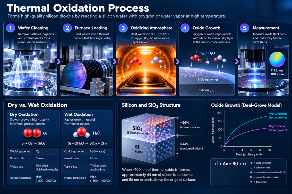
Step 1. Wafer Cleaning
Before oxidation begins, the wafer surface must be carefully cleaned.
Particles, organic residues, metallic contaminants, and unwanted surface films can interfere with oxide growth and electrical quality.
Cleaning helps prepare the silicon surface for controlled oxidation.
Step 2. Wafer Loading
The wafers are loaded into a thermal processing furnace.
Traditional batch furnaces can process multiple wafers simultaneously, while some thermal processes use single-wafer equipment.
The furnace provides controlled temperature and gas conditions.
Step 3. Temperature Control
The wafers are heated to an elevated temperature.
Conventional furnace oxidation commonly operates at approximately 800–1,100°C, although actual conditions depend on the application and equipment.
Temperature is a critical parameter because it strongly influences the oxidation rate.
Step 4. Oxidizing Gas Supply
Oxygen or water vapor is introduced into the process chamber.
These species react with silicon to form silicon dioxide.
The two major oxidation approaches are:
- Dry oxidation
- Wet oxidation
Step 5. Oxide Growth
Oxidizing species diffuse through the growing oxide and react at the silicon–oxide interface.
As oxidation continues, the oxide layer becomes thicker.
However, growth does not generally remain linear with time because the growing oxide increasingly limits oxidant transport.
Step 6. Cooling and Unloading
After reaching the target oxidation condition, the oxidizing atmosphere and temperature are controlled according to the process recipe.
The wafers are then cooled and unloaded.
The resulting oxide thickness and properties are measured before further processing.
Dry Oxidation vs. Wet Oxidation
The two most common thermal oxidation methods use different oxidizing species.
Dry Oxidation
Dry oxidation uses molecular oxygen.
The simplified chemical reaction is:
\[ Si + O_2 \rightarrow SiO_2 \]
Dry oxidation generally produces oxide more slowly than wet oxidation at comparable temperatures.
However, it is often preferred when high-quality electrical interfaces and precise thin-oxide control are important.
Wet Oxidation
Wet oxidation uses water vapor.
The simplified chemical reaction is:
\[ Si + 2H_2O \rightarrow SiO_2 + 2H_2 \]
Wet oxidation typically provides a faster oxide growth rate.
This can be useful when relatively thick oxide layers are required.
Dry vs. Wet Oxidation Comparison
| Parameter | Dry Oxidation | Wet Oxidation |
|---|---|---|
| Oxidizing species | O₂ | H₂O vapor |
| Growth rate | Slower | Faster |
| Typical strength | Thin oxide control and interface quality | Faster growth of thicker oxides |
| Common use | High-quality thin oxide applications | Thicker oxide applications |
| Process temperature | High | High |
Neither method is universally better.
The appropriate choice depends on the required oxide thickness, electrical properties, throughput, and process integration.
Why Oxide Thickness Control Matters
Semiconductor manufacturing requires oxide layers with carefully controlled thickness.
The required thickness can vary significantly depending on the application.
Some structures require extremely thin insulating layers, while others require much thicker oxide films.
Thickness affects characteristics such as:
- Electrical capacitance
- Insulation performance
- Breakdown behavior
- Masking effectiveness
- Device geometry
- Subsequent etching behavior
For this reason, oxidation time, temperature, ambient composition, and wafer condition must be controlled carefully.
The Deal–Grove Model
One of the most important theoretical models for thermal oxidation is the Deal–Grove model.
It describes silicon oxide growth using the combined effects of surface reaction and oxidant transport through the growing oxide.
A simplified expression is:
\[ x^2 + Ax = B(t+\tau) \]
Where:
- \(x\) = oxide thickness
- \(t\) = oxidation time
- \(A\) = parameter associated with the transition between growth regimes
- \(B\) = parabolic rate constant
- \(\tau\) = time offset accounting for initial oxide thickness
The model helps explain two important growth regimes.
Reaction-Limited Growth
For relatively thin oxide layers, the chemical reaction at the silicon–oxide interface can be the dominant limitation.
Oxide thickness may increase approximately linearly with time.
Diffusion-Limited Growth
As the oxide becomes thicker, oxidizing species must travel through a longer oxide layer before reaching the silicon interface.
Transport becomes increasingly important.
Oxide growth slows, and thickness can approach a square-root dependence on time.
The Deal–Grove model is particularly useful for conventional thermal oxidation, although additional models are needed to describe some ultrathin-oxide growth conditions accurately.
Thermal Oxidation Consumes Silicon
An important characteristic of thermal oxidation is that the process consumes part of the silicon wafer.
When silicon dioxide forms, oxygen atoms are incorporated into the material.
The oxide occupies a greater volume than the silicon consumed to produce it.
For conventional oxidation, approximately 44% of the final oxide thickness corresponds to consumed silicon, while the remaining thickness extends above the original silicon surface.
For example, forming approximately 100 nm of thermal oxide consumes about 44 nm of silicon.
This matters when controlling device dimensions and surface geometry.
Why the Silicon–Oxide Interface Matters
One reason silicon became so successful in semiconductor manufacturing is the ability to form a useful insulating oxide directly on its surface.
However, the quality of the interface between silicon and silicon dioxide is extremely important.
Interface defects and trapped charges can influence electrical behavior.
Potential consequences include:
- Threshold voltage instability
- Increased leakage
- Reduced carrier mobility
- Reliability degradation
Careful oxidation and subsequent thermal treatments can help improve interface properties.
This is particularly important for MOS device structures.
Thermal Oxidation in MOS Transistors
A traditional MOS transistor uses a gate electrode separated from silicon by a thin insulating layer.
Historically, silicon dioxide served as this gate dielectric.
The structure can be simplified as:
Gate Electrode
↓
Gate Dielectric (SiO₂)
↓
Silicon Channel
The dielectric allows an electric field from the gate to control the channel without requiring direct electrical contact between the gate and silicon.
This principle is fundamental to MOS transistor operation.
As transistor dimensions became smaller, conventional silicon dioxide gate dielectrics faced increasing leakage challenges.
Advanced technologies therefore adopted high-k dielectric materials and metal gate electrodes.
Nevertheless, silicon oxide and carefully engineered interfacial layers remain relevant in semiconductor device fabrication.
Thermal Oxidation as a Masking Process
Silicon dioxide can also serve as a masking material.
For example, an oxide layer may protect selected silicon regions during subsequent processing.
Photolithography and etching can remove oxide from chosen areas while leaving other regions covered.
This allows manufacturers to control which regions are exposed to later processes.
Historically, oxide masking was particularly important in selective diffusion and other silicon processing steps.
Thermal Oxidation vs. Oxide Deposition
Silicon dioxide can be formed by thermal oxidation or deposited using processes such as CVD.
Although both approaches produce oxide-containing films, their manufacturing mechanisms are different.
| Thermal Oxidation | Oxide Deposition |
|---|---|
| Silicon reacts with oxygen or steam | Material is supplied through deposition chemistry |
| Consumes silicon substrate | Generally adds material onto a surface |
| Growth occurs at the silicon–oxide interface | Film forms on exposed surfaces |
| Requires an oxidizable silicon surface | Can coat various compatible substrates |
| Often produces a high-quality Si/SiO₂ interface | Useful for broader film integration |
Thermal oxidation is especially useful when a controlled silicon–oxide interface is required.
Deposition becomes important when oxide must be formed on other materials or complex structures.
For a broader explanation of deposited semiconductor films, see:
💻 Semiconductor #7 — How Thin Film Deposition Builds Semiconductor Devices Layer by Layer
Oxidation Equipment and Furnace Technology
Thermal oxidation is commonly performed using controlled high-temperature processing equipment.
Typical system components include:
- Process tube or reaction chamber
- Heating system
- Wafer carrier
- Oxygen supply
- Water vapor generation or delivery system
- Temperature monitoring
- Gas flow control
- Exhaust system
- Automated wafer handling
Batch furnaces are widely associated with thermal oxidation because they can process multiple wafers under controlled conditions.
Different equipment configurations are selected according to wafer size, throughput, temperature uniformity, contamination requirements, and process objectives.
Why Temperature Uniformity Matters
Oxidation rate is strongly temperature-dependent.
If wafers experience different temperatures, their oxide growth rates may differ.
This can create thickness variation between wafers or across a wafer.
Manufacturers therefore carefully control:
- Furnace temperature distribution
- Wafer loading conditions
- Gas flow
- Process time
- Heating and cooling profiles
Stable thermal processing is essential for repeatable oxide thickness.
Contamination Control in Thermal Oxidation
Thermal oxidation takes place at elevated temperatures, making contamination control especially important.
Unwanted impurities may influence oxide properties or the silicon–oxide interface.
Potential contamination sources include:
- Process gases
- Furnace components
- Wafer handling
- Residual chemicals
- Metallic particles
- Previous process residues
High-purity gases, suitable chamber materials, cleaning procedures, and controlled wafer handling help reduce contamination risk.
Thermal Oxidation and Advanced Semiconductor Manufacturing
Thermal oxidation remains an important process, but its applications have evolved.
Advanced logic manufacturing uses increasingly complex material stacks and device architectures.
High-k dielectrics, metal gates, and three-dimensional transistor structures have changed how insulating layers are formed and integrated.
Nevertheless, thermal oxidation remains relevant in applications such as:
- Selected silicon surface preparation processes
- Oxide masking
- Sacrificial oxide formation
- Certain isolation-related process steps
- Interfacial oxide engineering
- Specialized semiconductor devices
The exact role depends on the technology node and process architecture.
Thermal Oxidation in Power Semiconductors
Power semiconductor devices often require different structures and operating characteristics from advanced logic chips.
Silicon-based power MOSFETs can use thermally grown oxide layers in gate structures and other applications.
Oxide thickness, interface quality, and electrical reliability are especially important because power devices may operate under demanding voltage and temperature conditions.
Thermal oxidation also plays an important role in silicon carbide device manufacturing, although SiC oxidation presents additional interface-quality challenges compared with conventional silicon oxidation.
The Future of Thermal Oxidation
As semiconductor manufacturing evolves, oxidation technology continues to focus on tighter process control and improved interface properties.
Important development areas include:
- Improved ultrathin oxide control
- Lower defect density
- Better interface engineering
- Reduced contamination
- Advanced thermal processing
- Integration with high-k materials
- Improved process monitoring
- Specialized oxidation for power semiconductor materials
Although newer dielectric materials have changed some applications, understanding thermal oxidation remains essential for understanding semiconductor manufacturing.
Key Takeaways
- Thermal oxidation forms silicon dioxide by reacting silicon with oxygen or water vapor at high temperature.
- Dry oxidation generally provides slower growth and is often used where precise thin-oxide control and interface quality are important.
- Wet oxidation provides faster oxide growth and is useful for thicker films.
- Thermal oxidation consumes part of the silicon substrate.
- Oxide growth is influenced by chemical reaction kinetics and oxidant transport.
- The Deal–Grove model describes conventional oxide growth behavior.
- Silicon dioxide has historically played a central role in MOS transistor development.
- Oxide thickness, interface quality, temperature uniformity, and contamination control are critical process parameters.
- Thermal oxidation remains relevant in modern semiconductor and power device manufacturing.
Frequently Asked Questions
What is thermal oxidation in semiconductor manufacturing?
Thermal oxidation is a high-temperature process that forms silicon dioxide by reacting silicon with oxygen or water vapor.
What is the difference between dry and wet oxidation?
Dry oxidation uses oxygen and generally grows oxide more slowly, while wet oxidation uses water vapor and typically provides faster oxide growth.
Why is silicon dioxide important?
Silicon dioxide provides electrical insulation, surface protection, masking capabilities, and useful interface properties for silicon semiconductor devices.
Does thermal oxidation consume silicon?
Yes. Thermal oxidation converts part of the silicon substrate into silicon dioxide. Approximately 44 nm of silicon is consumed when forming 100 nm of conventional thermal oxide.
Is thermal oxidation still used in advanced semiconductor manufacturing?
Yes. Although advanced logic devices often use high-k gate dielectrics, thermal oxidation remains useful in selected oxide formation, surface preparation, masking, interface engineering, and specialized device processes.
What is the Deal–Grove model?
The Deal–Grove model describes conventional silicon oxidation kinetics by considering interface reaction and oxidant diffusion through the growing oxide.
📖 Semiconductor Learning Path
↓
Current: 💻 Semiconductor #11 | How Thermal Oxidation Grows Silicon Dioxide on a Wafer
↓
Next: 💻 Semiconductor #12 | How Chemical Vapor Deposition Builds Thin Films on Semiconductor Wafers
📚 Continue Reading
- 💻 Semiconductor #2 | Why Silicon Wafers Are the Foundation of Modern Chips
- 💻 Semiconductor #4 | Wafer Manufacturing: From Silicon Ingot to Wafer
- 💻 Semiconductor #5 | How Photolithography Creates Billions of Transistors
- 💻 Semiconductor #7 | How Thin Film Deposition Builds Semiconductor Devices Layer by Layer
- 💻 Semiconductor #10 | How Semiconductor Inspection & Metrology Find Nanometer-Scale Defects
References
Recommended primary technical sources:
- SEMI — Semiconductor Manufacturing and Thermal Processing
- Tokyo Electron (TEL) — Thermal Processing Systems
- ASM International — Vertical Furnace and Thermal Processing Technology
- IEEE Electron Devices Society — Silicon Dioxide and MOS Device Technology
The foundational academic reference for the oxidation model is:
ℹ️ About iAtlas
iAtlas is an independent publication covering batteries, semiconductors, OLED, advanced materials, AI, and global industrial trends.
We transform complex industrial developments into clear, reliable, and easy-to-understand insights.
Whether you’re following today’s industry news or building long-term expertise, iAtlas helps you understand not only what happened, but why it matters.
Technology creates change.
Insight creates opportunity.
— iAtlas