Hybrid Bonding May Arrive Later Than Expected in HBM
HBM4 Can Still Use Microbumps, but the Semiconductor Industry Is Already Preparing for the Next Packaging Transition
🧠 iAtlas Daily #52 | Semiconductor & Advanced Packaging | September 2026
For several years, HBM Hybrid Bonding appeared to be one of the most inevitable transitions in advanced semiconductor packaging.
As High Bandwidth Memory stacks became taller and interconnect pitches became smaller, conventional microbumps seemed to be approaching their physical limits.
The expectation was straightforward:
HBM3E
↓
HBM4
↓
Hybrid Bonding
But the transition is proving more complicated.
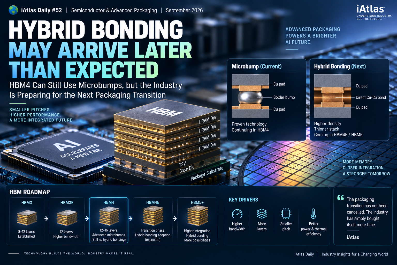
Changes to HBM package-height limits and continued improvements in microbump technology mean that HBM4 can remain with conventional bonding approaches longer than previously expected.
Hybrid bonding has not disappeared.
Instead, its mass adoption in HBM may be moving toward HBM4E, HBM5 and later generations.
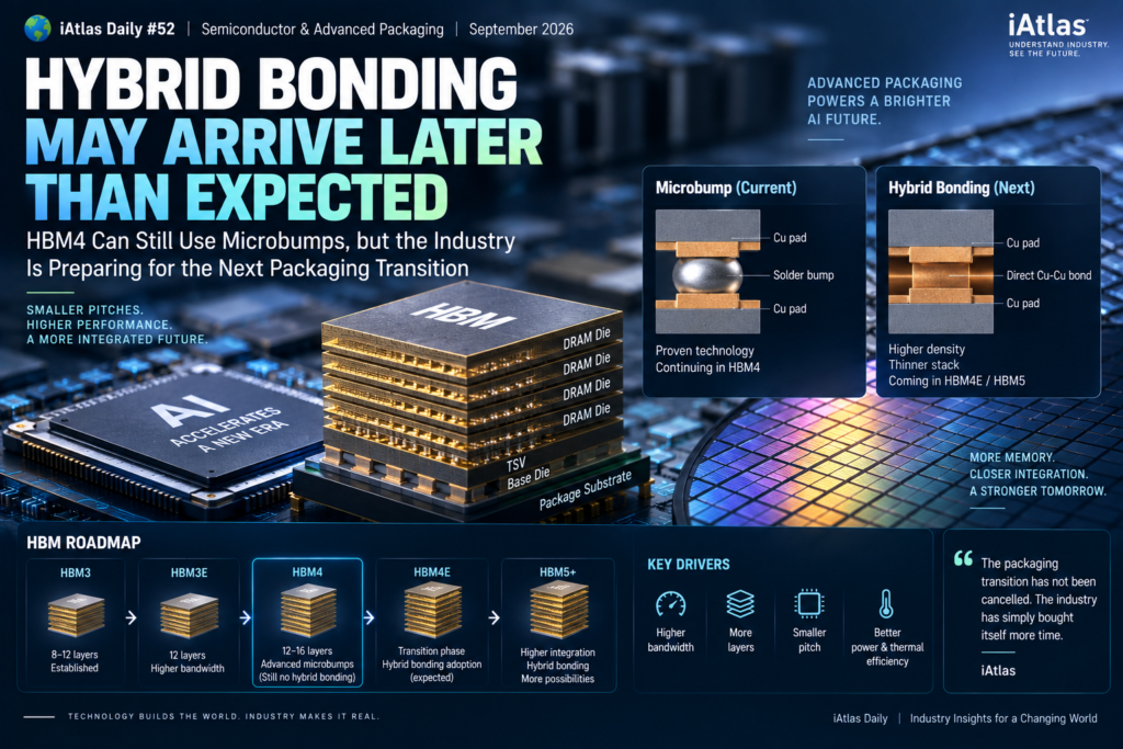
The packaging transition has not been cancelled. The industry has simply bought itself more time.
🧠 The Big Story
HBM is built by vertically stacking multiple DRAM dies.
Those dies must communicate through extremely dense vertical electrical connections.
Traditionally, the connection structure includes:
DRAM Die
↓
TSV
↓
Microbumps
↓
Next DRAM Die
As HBM stacks become taller, however, every micron matters.
More DRAM layers mean:
- greater package height
- more interconnections
- tighter pitches
- higher thermal density
- more difficult manufacturing
Hybrid bonding offers a potential solution because it eliminates conventional solder bumps and directly connects copper pads.
But semiconductor manufacturing rarely replaces an established process before it becomes necessary.
That is exactly what appears to be happening with HBM4.
📏 1. HBM Has a Height Problem
The fundamental challenge begins with geometry.
HBM performance increases partly by stacking more DRAM dies.
Earlier generations used relatively fewer layers.
The industry is now moving toward:
8-High
↓
12-High
↓
16-High
↓
Potentially even taller structures
But HBM packages must remain within standardized dimensional limits.
That creates a simple problem:
More DRAM Layers
Bonding Layers
Base Die
=
Taller HBM Package
Reducing the thickness of each bonding interface therefore becomes increasingly valuable.
This was one of the major reasons hybrid bonding attracted so much attention.
🔗 2. What Hybrid Bonding Changes
Conventional stacking uses microscopic solder bumps between dies.
Hybrid bonding removes those bumps.
Instead, extremely flat surfaces containing copper pads are aligned and bonded directly.
Microbump
Copper Pad
↓
Solder Bump
↓
Copper Pad
Hybrid Bonding
Copper
↕ Direct Connection
Copper
The advantages can include:
- smaller interconnect pitch
- higher connection density
- thinner stacks
- potentially better electrical performance
- improved power efficiency
- improved thermal characteristics
This makes the technology extremely attractive for 3D semiconductor integration.
SK hynix describes hybrid bonding as a foundational technology for future semiconductor performance as memory and logic become more tightly integrated.
🔬 3. But Hybrid Bonding Is Much Harder to Manufacture
Removing the solder bump sounds simple.
Manufacturing it is not.
Hybrid bonding requires two surfaces to be extraordinarily:
Flat
Clean
Smooth
Precisely aligned
A microscopic contaminant can interfere with bonding across multiple connections.
Chemical Mechanical Planarization — CMP — therefore becomes particularly important.
The surfaces must be prepared with extreme precision before bonding.
The process broadly becomes:
Wafer Preparation
↓
CMP
↓
Surface Cleaning
↓
Alignment
↓
Copper-to-Copper Bonding
↓
Inspection
This introduces demanding new requirements for equipment, contamination control and process integration.
📐 4. HBM4 Got More Vertical Space
One development changed the near-term calculation.
The HBM package-height limit was increased from approximately 720 μm to 775 μm.
That additional space gives memory manufacturers more flexibility when constructing taller HBM stacks.
Previously, the equation appeared to be:
16-Layer HBM
↓
Too Tall with Microbumps
↓
Hybrid Bonding Required
Now:
Higher Package Limit
Thinner Dies
Advanced Microbumps
↓
HBM4 Can Potentially Continue Without Hybrid Bonding
That changes the economics considerably.
💰 5. Why Replace Microbumps Before You Need To?
Semiconductor manufacturing technologies are not adopted simply because they are technically superior.
They must also make economic sense.
Microbump processes already have:
- established equipment
- established suppliers
- production experience
- mature process control
- known yield characteristics
Hybrid bonding requires new equipment and tighter manufacturing tolerances.
So if microbumps can still satisfy HBM4 requirements, manufacturers have an incentive to continue using them.
The decision becomes:
Microbump
Lower technological risk
Mature manufacturing
Existing infrastructure
versus
Hybrid Bonding
Higher interconnect density
Smaller pitch
Future scalability
Greater manufacturing complexity
For HBM4, the industry may still favor the first option.
⚙️ 6. Microbumps Are Still Getting Smaller
This does not mean conventional packaging technology has stopped advancing.
Quite the opposite.
The industry is working to push microbumps toward increasingly fine pitches and reduced heights.
The latest HBM generations are approaching interconnect dimensions that would once have been considered extremely aggressive.
This creates an interesting technology race:
Improve Microbumps
versus
Transition to Hybrid Bonding
Every improvement in conventional bonding delays the point at which the new technology becomes economically necessary.
This pattern is common in semiconductor manufacturing.
Older technologies often survive much longer than expected because engineers continue improving them.
🏭 7. SK hynix Is Preparing for Both Paths
SK hynix provides a good example.
The company continues developing hybrid bonding technology while also improving its established HBM stacking methods.
In an August 25 technical note, SK hynix emphasized that hybrid bonding becomes increasingly important as semiconductor architectures move toward greater integration between memory and logic.
But that does not necessarily mean every HBM4 product must immediately use it.
The strategy effectively becomes:
HBM4
Advanced conventional bonding
↓
HBM4E
Potential hybrid-bonding expansion
↓
HBM5
Hybrid bonding increasingly important
The exact timing will depend on package architecture, stack height, yield and economics.
🧩 8. TSMC Is Already Using Hybrid Bonding Elsewhere
There is another important distinction.
Hybrid bonding itself is not a future technology.
It is already in production.
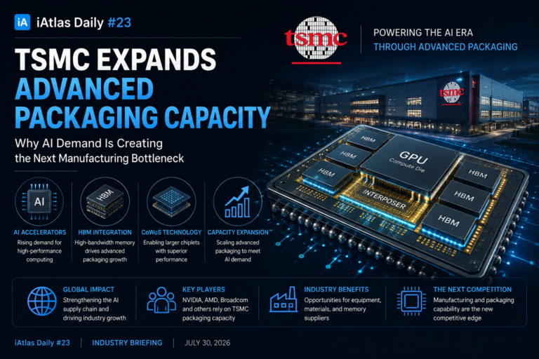
TSMC uses hybrid bonding in its SoIC — System on Integrated Chips — platform for advanced logic integration.
Its roadmap has moved bonding pitch from approximately 9 μm toward 6 μm, with still finer pitches planned.
This allows structures such as:
Logic Die
↕
Hybrid Bonding
↕
Logic / I/O Die
↓
CoWoS
↓
HBM
So advanced AI packages can already contain hybrid bonding even when the HBM stacks themselves still use microbumps.
That distinction is important.
🧱 9. Advanced Packaging Is Becoming a Combination of Technologies
The old view of semiconductor packaging was relatively simple.
Chip
↓
Package
↓
PCB
AI processors have changed that.
Modern packages increasingly combine:
GPU / Accelerator
Chiplets
HBM
Silicon Interposer
Advanced Substrate
Hybrid Bonding
Microbumps
A single package can therefore contain multiple interconnection technologies simultaneously.
Advanced packaging is becoming less like a single manufacturing process and more like a system-integration architecture.
🤝 10. Memory and Logic Are Moving Closer Together
This may ultimately be more important than the exact generation when hybrid bonding enters HBM.
SK hynix recently described the future of AI memory in terms of increasing integration between memory and logic.
Historically:
CPU / GPU
↔
Memory
were separate components connected through relatively long electrical paths.
The future increasingly moves toward:
Logic
↕
Memory
with tighter physical integration.
Hybrid bonding enables much denser vertical connections between different semiconductor dies.
That opens possibilities for:
- memory-on-logic
- logic inside memory architectures
- advanced chiplets
- 3D compute structures
- customized HBM
So hybrid bonding should not be viewed only as an HBM stacking technology.
It is part of the broader movement toward 3D semiconductor integration.
🌡️ 11. Thermal Management Becomes More Important Too
There is a trade-off.
Putting more semiconductor dies closer together improves communication.
But it also concentrates heat.
AI accelerators already operate at extremely high power levels.
HBM stacks sit physically close to these processors.
Future 3D structures could place memory and logic even closer.
The engineering challenge therefore becomes:
Higher Integration
↓
Shorter Interconnects
↓
Higher Performance
but also
↓
Greater Heat Density
This makes:
- thermal interface materials
- package design
- cooling
- heat spreading
- materials engineering
increasingly important parts of advanced packaging.
🛠️ 12. A New Equipment Market Is Emerging
Even if HBM hybrid bonding adoption arrives later than expected, equipment suppliers are already preparing.
Hybrid bonding requires specialized systems for:
CMP
Surface Preparation
Cleaning
Metrology
Alignment
Die Placement
Bonding
Inspection
Companies across the semiconductor-equipment industry are developing these technologies.
For die-to-wafer bonding in particular, throughput becomes critical because individual known-good dies must be aligned and placed with extreme precision.
Current commercial platforms are moving toward thousands of die placements per hour while simultaneously targeting increasingly fine alignment accuracy.
This creates a new equipment opportunity before hybrid bonding reaches full HBM volume.
🧪 13. Cleanliness Becomes a Technology Requirement
Hybrid bonding also illustrates an important semiconductor manufacturing principle:
As dimensions shrink, contamination becomes part of the technology itself.
A particle that would have been insignificant in older packaging can become catastrophic when interconnect pitches reach only a few micrometers.
That raises the importance of:
Cleanroom Control
Surface Cleaning
Particle Inspection
CMP
Wafer Handling
Process Environment
Packaging is therefore adopting manufacturing requirements historically associated more strongly with front-end wafer processing.
The boundary between front-end and back-end semiconductor manufacturing is becoming less distinct.
📈 14. HBM4E and HBM5 May Be the Real Turning Point
HBM4’s ability to remain with microbumps does not solve the scaling problem forever.
Future generations will continue pushing:
More Layers
More Bandwidth
Smaller Pitch
Higher Density
Lower Power
Eventually, conventional bonding approaches face physical limits.
That is why current industry roadmaps increasingly point toward later HBM generations as the more likely inflection point for hybrid bonding.
The likely transition is therefore not:
Microbump → Hybrid Bonding overnight
but:
Microbump
↓
Fine-Pitch Microbump
↓
Hybrid Bonding in Selected Products
↓
Broader Hybrid Bonding Adoption
Technology transitions are usually evolutionary before they become revolutionary.
🧩 Why This Matters
The HBM Hybrid Bonding transition reveals several important lessons about semiconductor manufacturing.
Better technology does not always win immediately.
Manufacturing cost and yield matter just as much as technical capability.
Existing technologies continue improving.
Fine-pitch microbumps are extending the life of conventional HBM stacking.
Hybrid bonding is still coming.
Its role may simply shift toward HBM4E, HBM5 and deeper memory-logic integration.
Packaging is becoming semiconductor manufacturing.
Advanced packaging now requires extreme precision, cleanliness and process control.
Equipment opportunities arrive before full adoption.
Toolmakers must build production capability before new architectures reach mass volume.
🔭 What to Watch
HBM4 Yield
If conventional bonding achieves strong yields at 12- and 16-layer configurations, hybrid bonding adoption could remain gradual.
HBM4E
This may become the first important transition point.
HBM5
Higher stacks and tighter pitches could make hybrid bonding increasingly difficult to avoid.
SK hynix
Watch how its advanced MR-MUF technology evolves alongside hybrid-bonding development.
Samsung Electronics
Samsung’s packaging roadmap increasingly combines memory, foundry and advanced logic technologies.
TSMC SoIC
Logic-side hybrid bonding adoption will provide valuable production experience before memory volumes expand.
Bonding Equipment
Applied Materials, Besi, ASMPT, EV Group and Korean equipment suppliers are worth watching as the tool ecosystem develops.
🧭 iAtlas Insight
Hybrid bonding illustrates why semiconductor technology roadmaps rarely move in straight lines.
The industry believed HBM4 might force a major packaging transition.
Engineers instead found more room.
They increased the package-height limit.
They continued shrinking microbumps.
They improved existing processes.
And they postponed the point at which the new technology becomes unavoidable.
But the fundamental scaling problem remains.
More Memory
↓
More Layers
↓
More Connections
↓
Smaller Pitch
↓
Greater Integration
Eventually, solder bumps cannot shrink forever.
Hybrid bonding may arrive later than expected in HBM — but the semiconductor industry’s direction toward direct copper-to-copper integration has not changed.
The question is increasingly not whether hybrid bonding will become important.
It is when the economics finally make it unavoidable.
📚 Related Articles
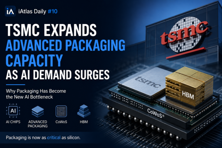
📰 iAtlas Daily #10: TSMC Advanced Packaging Expansion Signals the Next AI Boom
Why advanced packaging capacity has become a critical part of the AI semiconductor supply chain.
📰 iAtlas Daily #34: Korea Semiconductor Fund Targets the Supply Chain
How Korea is strengthening its semiconductor materials, equipment and manufacturing ecosystem.
🔗 References
SK hynix — Hybrid Bonding: A Foundational Technology for Semiconductor Performance
SK hynix — Memory and Logic Integration at TSMC Technology Symposium 2026
Tom’s Hardware — The State of Hybrid Bonding in 2026
About iAtlas
iAtlas is an independent publication covering batteries, semiconductors, OLED, advanced materials, AI, and global industrial trends.
We transform complex industrial developments into clear, reliable, and easy-to-understand insights.
Whether you’re following today’s industry news or building long-term expertise, iAtlas helps you understand not only what happened, but why it matters.
Technology creates change.
Insight creates opportunity.
— iAtlas