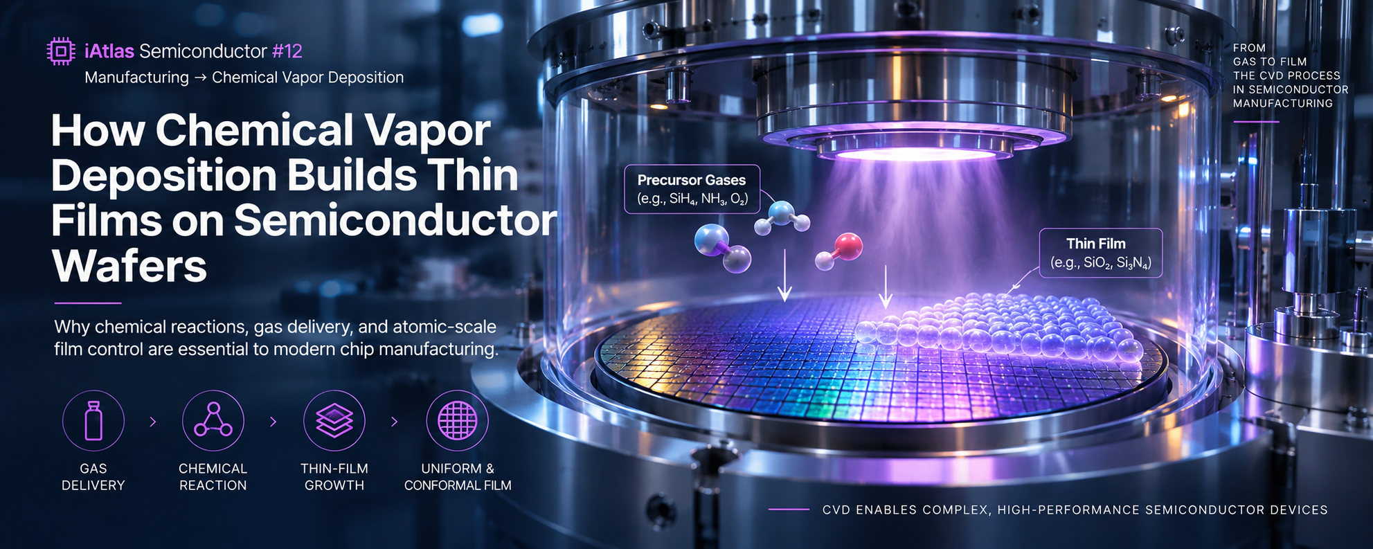
How Chemical Vapor Deposition Builds Thin Films on Semiconductor Wafers
💻 iAtlas Semiconductor #12 | 📘 Manufacturing → Chemical Vapor Deposition
Introduction
Modern semiconductor chips are built from far more than silicon.
Inside a semiconductor device, numerous thin films perform essential functions. Some electrically isolate neighboring structures. Others help form transistors, protect delicate surfaces, or provide materials needed for electrical connections.
Many of these layers are only a few nanometers thick.
Producing them consistently across an entire silicon wafer is one of the fundamental challenges of semiconductor manufacturing.
One of the most important technologies used to accomplish this is Chemical Vapor Deposition (CVD).
CVD uses gaseous chemicals to create solid thin films through controlled chemical reactions. By carefully managing temperature, pressure, gas composition, and reaction conditions, manufacturers can deposit materials with precisely engineered properties.
As semiconductor structures become smaller, taller, and more complex, thin-film deposition becomes increasingly important.
Understanding CVD therefore helps explain not only how chips are manufactured, but also why advanced semiconductor equipment and materials are critical to future device performance.
1. What Is Chemical Vapor Deposition?
Chemical Vapor Deposition is a semiconductor manufacturing process in which gaseous precursors react or decompose to form a solid material on a substrate.
In simple terms, CVD transforms selected gases into a thin solid layer on a wafer.
The process generally involves three elements:
- Precursor gases: Chemicals containing the elements needed to form the film.
- Reaction energy: Usually thermal energy, plasma energy, or a combination of both.
- Substrate surface: The wafer on which the deposited material forms.
For example, silicon-containing precursor gases can be used to deposit silicon-based films, while other combinations can produce insulating or conductive materials.
The resulting thin films may serve as electrical insulators, protective barriers, structural layers, or components of advanced semiconductor devices.
Unlike coating methods that simply spread a liquid over a surface, CVD relies on chemical reactions that occur at or near the wafer surface.
This distinction gives CVD important advantages in film composition, uniformity, and coverage of complex structures.
2. Why Thin Films Are Essential in Semiconductor Manufacturing
A semiconductor chip contains many different materials arranged in carefully designed structures.
Each material performs a particular function.
| Thin-film material | Typical semiconductor function |
| Silicon Dioxide (SiO₂) | Electrical insulation, dielectric layers, and protective films |
| Silicon Nitride (Si₃N₄) | Insulation, passivation, diffusion barriers, and etch-stop layers |
| Polysilicon | Conductive or structural layers in selected device architectures |
| Tungsten (W) | Contacts, plugs, and selected conductive structures |
| Specialized dielectric films | Electrical isolation and capacitance control |
The properties of these films influence how well a semiconductor device operates.
For example, an insulating film must prevent unwanted current leakage, while a conductive film must provide reliable electrical connections.
Film thickness is equally important.
A layer that is too thin may fail to provide sufficient insulation. A layer that is too thick may interfere with the intended device dimensions or electrical characteristics.
Manufacturers must therefore control not only which materials are deposited, but also their thickness, composition, uniformity, and defect levels.
CVD is one of the technologies that makes this possible.
3. How Chemical Vapor Deposition Works
Although CVD equipment varies by application, the fundamental process follows a common sequence.
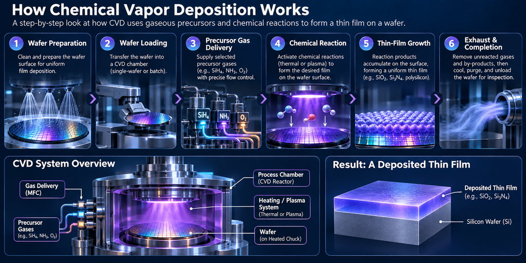
Step 1. Wafer Preparation
Before deposition begins, the wafer must meet the cleanliness and surface-condition requirements of the process.
Particles, organic residues, or unwanted surface contamination can interfere with film formation.
Depending on the application, the wafer may undergo wet cleaning, dry cleaning, or other surface preparation.
Step 2. Wafer Loading
The wafer is transferred into a deposition chamber.
Some CVD systems process one wafer at a time, while batch systems can process multiple wafers simultaneously.
The chamber provides a controlled environment for the chemical reactions.
Step 3. Precursor Gas Delivery
Selected precursor gases enter the chamber through a gas delivery system.
Mass flow controllers regulate the flow rates of individual gases.
The choice of precursors depends on the film material, deposition chemistry, and required film properties.
Step 4. Chemical Reaction
Energy is supplied to initiate or sustain the chemical reactions.
In thermal CVD, heat provides the necessary reaction energy.
In plasma-enhanced CVD, energetic species generated by plasma help drive reactions at lower substrate temperatures than many corresponding thermal processes.
Reaction products form on the wafer surface, while gaseous by-products are removed through the exhaust system.
Step 5. Thin-Film Growth
The deposited material accumulates on the wafer.
Film growth depends on several interacting factors, including precursor transport, surface reactions, temperature, pressure, and the geometry of the structures being coated.
The objective is to achieve the required thickness and film properties across the wafer.
Step 6. Exhaust and Process Completion
Unreacted precursor gases and gaseous by-products are removed through the chamber exhaust and appropriate gas-treatment systems.
After deposition, the wafer may undergo cooling, purging, transfer, and inspection.
Metrology equipment can then evaluate film thickness, uniformity, composition, or other characteristics.
The central challenge of CVD is controlling a chemical reaction well enough to create the same high-quality material across millions or billions of microscopic device features.
4. Major Types of Chemical Vapor Deposition
CVD is not a single process.
Several variations have been developed to accommodate different materials, device structures, and manufacturing requirements.
4.1 Atmospheric Pressure CVD (APCVD)
Atmospheric Pressure Chemical Vapor Deposition operates at or near atmospheric pressure.
It can offer relatively high deposition rates and simpler pressure-management requirements.
However, gas-phase reactions and transport conditions can make film uniformity and particle control challenging for certain applications.
APCVD remains relevant in selected semiconductor and industrial coating processes.
4.2 Low Pressure CVD (LPCVD)
Low Pressure Chemical Vapor Deposition operates under reduced pressure.
Lower pressure changes gas transport and reaction conditions, often helping improve film uniformity and step coverage for suitable chemistries.
LPCVD is commonly associated with films such as silicon nitride, polysilicon, and certain silicon dioxide layers.
Many LPCVD processes use relatively high temperatures, which must be compatible with the materials already present on the wafer.
4.3 Plasma-Enhanced CVD (PECVD)
Plasma-Enhanced Chemical Vapor Deposition uses plasma to generate reactive chemical species.
This allows many films to be deposited at lower substrate temperatures than comparable thermal CVD processes.
PECVD is widely used for dielectric films, passivation layers, and other applications where thermal budgets are important.
However, plasma conditions can influence film density, hydrogen incorporation, stress, and possible surface damage.
4.4 High-Density Plasma CVD (HDP-CVD)
High-Density Plasma CVD uses a dense plasma environment and can combine deposition with ion-assisted effects.
It has been used for dielectric gap-fill applications, particularly in semiconductor structures where conventional deposition may leave voids.
Its suitability depends on the feature geometry, material, and integration requirements.
Comparison of Major CVD Technologies
| Technology | Main characteristic | Typical advantage | Important consideration |
|---|---|---|---|
| APCVD | Near-atmospheric pressure | Potentially high deposition rate | Gas-phase reactions and uniformity |
| LPCVD | Reduced pressure, thermal reactions | Uniformity and step coverage | Often high process temperature |
| PECVD | Plasma-assisted reactions | Lower-temperature processing | Film properties and plasma effects |
| HDP-CVD | High-density plasma | Selected gap-fill capabilities | Ion effects and process complexity |
The best deposition method depends on the application rather than a single universal performance ranking.
5. CVD vs. Thermal Oxidation
Thermal Oxidation and CVD can both produce silicon dioxide films, but they work differently.
| Characteristic | Thermal Oxidation | CVD |
| Basic mechanism | Silicon reacts with oxygen or steam | Gaseous precursors react to deposit a solid film |
| Silicon substrate consumption | Yes, when growing SiO₂ on silicon | Generally not required for film formation |
| Material flexibility | Primarily thermal oxide on silicon | Many dielectric, semiconductor, and conductive materials |
| Substrate flexibility | Requires an oxidizable surface for oxide growth | Can deposit on a variety of compatible surfaces |
| Common applications | High-quality Si/SiO₂ interfaces, oxide layers | Dielectrics, barriers, structural and conductive films |
One of the most important differences is how the oxide forms.
During thermal oxidation of silicon, the oxide grows by consuming part of the silicon substrate.
During silicon dioxide CVD, the deposited film is formed from externally supplied precursor chemicals.
This gives CVD greater flexibility in depositing films over existing materials and device structures.
However, thermally grown silicon dioxide can offer particularly favorable interface properties on silicon, making it valuable for applications where the silicon–oxide interface is critical.
Neither technology replaces the other in every situation.
Both remain important parts of semiconductor manufacturing.
6. CVD vs. PVD vs. ALD
CVD is also one of several major thin-film deposition technologies.
Three commonly discussed methods are Chemical Vapor Deposition, Physical Vapor Deposition, and Atomic Layer Deposition.
CPO Supply Chain 101 – Jason’s Chips
CVD
Chemical reactions form a solid film from gaseous precursors.
PVD
Physical processes transfer material from a source to the wafer.
ALD
Sequential, self-limiting surface reactions enable precise layer control.
| Method | Main mechanism | Key strength |
|---|---|---|
| CVD | Chemical reactions involving gaseous precursors | Versatile material deposition |
| PVD | Physical transfer of material | Important for many metallic and conductive films |
| ALD | Sequential self-limiting surface reactions | Excellent thickness control and conformality for suitable processes |
ALD is often considered a specialized form of chemical vapor deposition, but it is commonly discussed as a separate manufacturing category because of its distinct reaction sequence.
The differences become especially important when manufacturers must coat deep trenches, narrow openings, or complex three-dimensional structures.
7. Why Film Uniformity and Conformality Matter
Two important performance measures in thin-film deposition are uniformity and conformality.
Uniformity describes how consistently the film thickness or other properties are maintained across a wafer or a batch of wafers.
Conformality describes how consistently the film coats different surfaces of a three-dimensional feature.
For example, a film deposited over a trench may cover its top surface, sidewalls, and bottom with different thicknesses.
If the coating is too thin along the sidewalls, the device may experience insulation failures or other performance problems.
As semiconductor devices increasingly use three-dimensional architectures, conformality becomes more challenging.
This is particularly relevant to technologies such as:
- 3D NAND memory structures
- Advanced transistor architectures
- High-aspect-ratio trenches and holes
- Complex dielectric and barrier layers
- Advanced interconnect structures
Conformality depends on the deposition chemistry, reaction conditions, and feature geometry. Conventional CVD can provide excellent step coverage in some applications, while ALD is often selected when highly conformal ultrathin films are required.
8. The Importance of Temperature, Pressure, and Gas Flow
CVD performance depends on the precise control of multiple process variables.
Temperature
Temperature influences chemical reaction rates, surface mobility, and film properties.
Insufficient temperature may prevent reactions from proceeding efficiently.
Excessive temperature can cause unwanted reactions, affect film stress, or damage temperature-sensitive device structures.
Pressure
Chamber pressure affects gas transport, collision behavior, and reaction conditions.
Different pressure regimes are used to achieve particular deposition characteristics.
Gas Flow
Precursor delivery must remain stable and repeatable.
Flow variations can influence film thickness, composition, and uniformity.
Precursor Chemistry
The precursor determines which chemical species are available to form the film.
Its volatility, thermal stability, reactivity, and by-products all influence process design.
Chamber Cleanliness
Particles and unwanted deposits can generate defects.
CVD chambers therefore require appropriate cleaning, maintenance, and contamination-control procedures.
Together, these variables explain why deposition systems are sophisticated pieces of semiconductor manufacturing equipment rather than simple gas-heating chambers.
9. Why Precursor Materials Are Important
A precursor is a chemical that supplies the elements needed to form a deposited material.
The selection of precursor chemistry strongly affects the deposition process.
An effective precursor generally needs suitable volatility, stability during delivery, sufficient reactivity under process conditions, and acceptable contamination characteristics.
For example, silicon-containing precursors can be used to deposit silicon-based films, while metal-containing precursors are used for selected metallic or compound films.
However, precursor behavior can create practical challenges.
Some chemicals are sensitive to moisture or oxygen. Others are corrosive, toxic, flammable, or prone to decomposition.
As a result, precursor storage and delivery may require carefully controlled conditions, including appropriate temperature management, sealed handling, compatible materials, and gas safety systems.
The requirements depend on the specific chemical.
This creates an important connection between semiconductor materials and equipment engineering.
Advanced deposition performance depends not only on the reactor, but also on the purity, stability, and controlled delivery of the chemicals entering it.
10. How CVD Equipment Supports Semiconductor Manufacturing
A modern CVD system contains multiple subsystems that work together.
| Equipment subsystem | Main function |
| Process Chamber | Provides a controlled deposition environment |
| Gas Delivery System | Supplies and regulates precursor and process gases |
| Heating / Plasma System | Provides reaction energy |
| Vacuum and Pressure Control | Maintains required process pressure |
| Wafer Handling System | Transfers wafers between modules |
| Exhaust / Abatement | Removes and treats process gases and by-products |
| Process Control Software | Monitors and controls deposition conditions |
These systems must operate together with high repeatability.
Even small variations in gas delivery, temperature distribution, or chamber condition can affect film quality.
Equipment manufacturers therefore invest heavily in process control, chamber design, and contamination management.
11. Leading Companies in CVD Technology
Several major semiconductor equipment manufacturers provide deposition technologies used across the industry.
Applied Producer XP Pioneer CVD
Applied Materials
Provides a broad portfolio of semiconductor deposition equipment, including CVD-related technologies used for dielectric and conductive films.
Lam Research 科林研發以 ALTUS® Halo 實現鉬的原子層沉積 開啟半導體金屬化的新時代 | 蕃新聞
Lam Research
Develops deposition and related process technologies for advanced semiconductor manufacturing, including complex device structures.
Products and Services(semiconductor production process) | Tokyo Electron Ltd.
Tokyo Electron
Supplies semiconductor manufacturing systems including thermal processing and deposition technologies.
ASM International
Specializes in advanced deposition technologies, including epitaxy, ALD, and selected CVD-related processes.
These companies illustrate how semiconductor deposition is supported by a global ecosystem of equipment manufacturers, chemical suppliers, component manufacturers, and process developers.
12. Why CVD Is Becoming More Important
Semiconductor manufacturing is becoming more complex.
For decades, chip development was strongly associated with shrinking transistor dimensions.
Today, performance improvements increasingly depend on sophisticated materials, three-dimensional structures, and advanced integration techniques.
These changes create new challenges for thin-film deposition.
More Complex Transistors
Advanced transistor architectures require precise materials and interfaces across increasingly complex geometries.
Three-Dimensional Memory
3D NAND and other memory technologies rely on repeated material layers and high-aspect-ratio structures.
Advanced Packaging
Certain packaging and integration processes require specialized dielectric, barrier, and other deposited films.
New Materials
Semiconductor manufacturers continue to explore materials with improved electrical, thermal, or mechanical properties.
Each new material can require different precursor chemistry, deposition equipment, and process conditions.
Consequently, deposition technology is not merely a supporting manufacturing step.
It is an important enabler of continued semiconductor innovation.
Key Takeaways
1. CVD forms thin films through chemical reactions involving gaseous precursors. It is used to deposit insulating, semiconductor, and selected conductive materials.
2. Different CVD methods serve different manufacturing requirements. LPCVD, PECVD, APCVD, and HDP-CVD use different pressure and energy conditions.
3. Film quality depends on precise process control. Temperature, pressure, gas flow, precursor chemistry, and chamber conditions all influence deposition results.
4. Three-dimensional semiconductor structures increase deposition challenges. Uniformity, conformality, and material properties are increasingly important.
5. CVD connects semiconductor equipment with advanced materials. Reliable precursor supply and controlled chemical reactions are essential to successful manufacturing.
Frequently Asked Questions
What is the main purpose of CVD in semiconductor manufacturing?
CVD is used to deposit thin films that provide electrical insulation, conductivity, protection, or structural functions within semiconductor devices.
What is the difference between CVD and PVD?
CVD forms films through chemical reactions involving gaseous precursors, while PVD transfers material through physical processes such as sputtering or evaporation.
Why is PECVD widely used?
PECVD enables many deposition reactions at relatively low substrate temperatures, making it useful when the materials already present on a wafer cannot tolerate higher thermal budgets.
Can CVD deposit silicon dioxide?
Yes. Silicon dioxide can be deposited using appropriate CVD precursor chemistry. This differs from thermal oxidation, which forms silicon dioxide by reacting silicon with oxygen or steam.
Is ALD the same as CVD?
ALD belongs to the broader family of chemically driven vapor deposition methods, but its sequential, self-limiting surface reactions distinguish it from conventional continuous-flow CVD.
📖 Semiconductor Learning Path
PREVIOUS · #11
How Thermal Oxidation Grows Silicon Dioxide on a Wafer
Understand how silicon reacts with oxygen or steam to form high-quality insulating oxide layers.
CURRENT · #12
Current article
How Chemical Vapor Deposition Builds Thin Films on Semiconductor Wafers
NEXT · #13
How Physical Vapor Deposition Creates Thin Films for Semiconductor Chips
Explore sputtering, evaporation, and the role of physical deposition in semiconductor manufacturing.
📚 Continue Reading
- How Thin Film Deposition Builds Semiconductor Devices Layer by Layer — iAtlas Semiconductor #7
- How Plasma Etching Shapes Semiconductor Devices — iAtlas Semiconductor #6
- How CMP Creates an Ultra-Flat Semiconductor Surface — iAtlas Semiconductor #9
- How Semiconductor Inspection & Metrology Find Nanometer-Scale Defects — iAtlas Semiconductor #10
References
The following are official manufacturer resources for further reading. Their product and technology pages may change over time.
- Applied Materials — Semiconductor Manufacturing and Deposition Technologies
- Lam Research — Deposition and Semiconductor Processing
- Tokyo Electron — Semiconductor Production Equipment
- ASM — Advanced Semiconductor Deposition Technologies
- SEMI — Semiconductor Manufacturing Industry Resources
ℹ️ About iAtlas
iAtlas is an independent publication covering batteries, semiconductors, OLED, advanced materials, AI, and global industrial trends.
We transform complex industrial developments into clear, reliable, and easy-to-understand insights.
Whether you’re following today’s industry news or building long-term expertise, iAtlas helps you understand not only what happened, but why it matters.
Technology creates change.
Insight creates opportunity.
— iAtlas