Taiwan Is Building an Advanced Packaging Ecosystem Around TSMC
Kaohsiung’s New Baipu Industrial Park Shows Why Advanced Packaging Is Becoming a Strategic Layer of the Semiconductor Industry
🔲 iAtlas Daily #64 | Advanced Packaging & Semiconductor Manufacturing | September 2026
For decades, semiconductor manufacturing was dominated by one fundamental race:
Make Transistors Smaller
Smaller transistors enabled:
More Computing Power
Higher Density
Better Energy Efficiency
and:
More Advanced Chips
That race is not over.
But another race is becoming increasingly important.
How do we connect multiple advanced chips together?
Modern processors increasingly combine:
Logic
HBM
I/O
Chiplets
Accelerators
into highly integrated systems.
That means semiconductor performance increasingly depends not only on the transistor—
but also on the:
Package
Taiwan’s latest semiconductor investment reflects this shift.
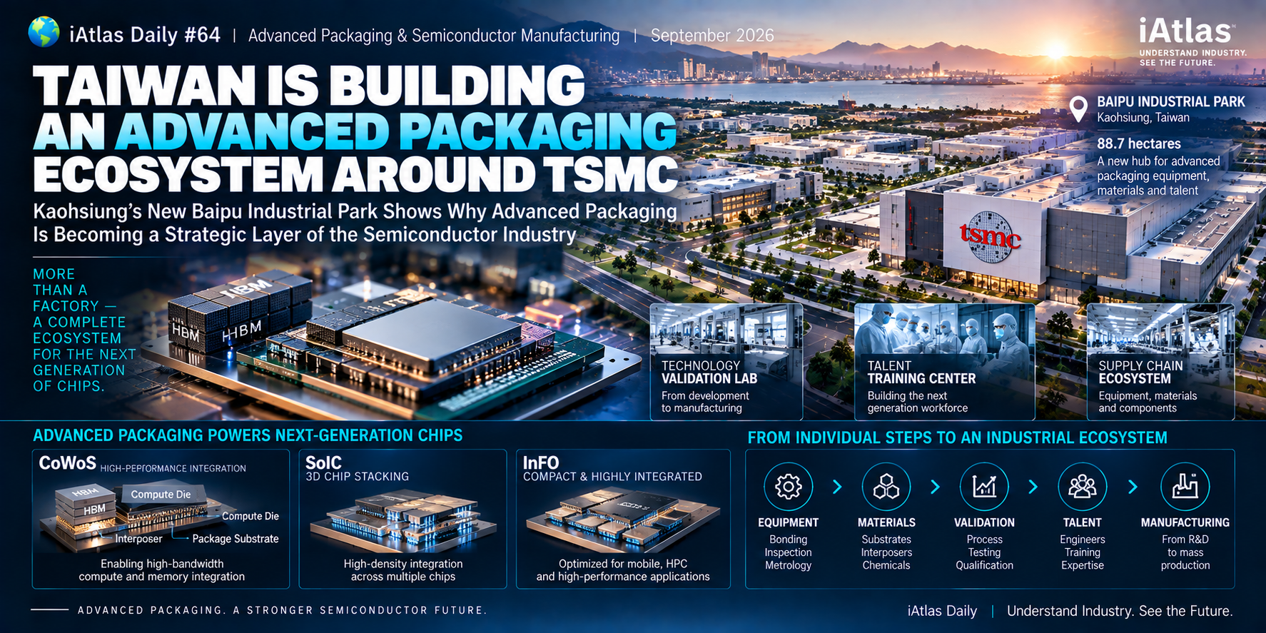
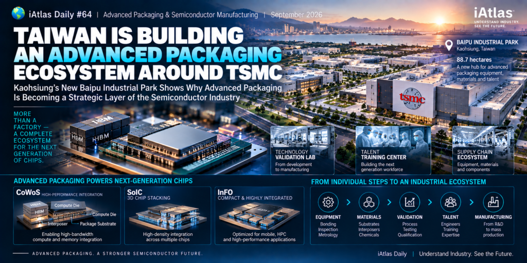
On September 21, construction began on the Baipu Industrial Park in Kaohsiung, a new industrial cluster focused heavily on advanced-packaging equipment and its supporting supply chain.
TSMC will establish a:
Technology Validation Laboratory
and:
Talent Training Center
inside the ecosystem, with operations targeted for the fourth quarter of 2029. Reuters
The project represents something larger than another industrial park.
It illustrates the transition:
Packaging as a Manufacturing Step
↓
Packaging as a Technology
↓
Packaging as a Performance Driver
↓
Packaging as an Industrial Ecosystem
The future of semiconductor performance will not be determined only by how small a transistor becomes. It will increasingly depend on how effectively multiple chips can be integrated into one system.
🌏 The Big Story
Taiwan already occupies one of the most important positions in global semiconductor manufacturing.
TSMC dominates leading-edge foundry manufacturing.
ASE Technology is one of the world’s largest semiconductor packaging and testing companies.
And a dense network of:
Equipment Suppliers
Materials Companies
Component Manufacturers
Engineers
and:
Research Institutions
supports the broader ecosystem.
Now Taiwan wants to deepen another layer.
Advanced Packaging
The new Baipu Industrial Park covers approximately 88.7 hectares, including around 53 hectares of industrial land.
Kaohsiung authorities say roughly 25 hectares will specifically target advanced semiconductor back-end equipment and related supply-chain companies. KCG
The goal is not simply to provide factory space.
Taiwan’s Ministry of Economic Affairs describes Baipu as a cluster for:
Advanced Packaging Materials
Equipment R&D
Testing & Validation
and:
Technology Deployment. Invest Taiwan
That distinction is important.
Taiwan is not simply adding packaging capacity.
It is trying to build:
An Advanced Packaging Ecosystem
🧩 1. First, What Is Semiconductor Packaging?
After semiconductor circuits are fabricated on a wafer, individual chips eventually need to be:
Separated
↓
Connected
↓
Protected
↓
Tested
↓
Integrated into Electronic Systems
Traditionally, packaging was often considered the final stage of semiconductor manufacturing.
The simplified industry structure looked like:
Chip Design
↓
Wafer Fabrication
↓
Packaging
↓
Testing
↓
Electronic Product
Packaging was essential.
But it was often perceived as less technologically important than wafer fabrication.
That perception is changing rapidly.
📦 2. Traditional Packaging Was Mostly About Protecting the Chip
At its most basic level, a semiconductor package performs several functions.
It protects the silicon die.
It provides electrical connections.
It helps manage heat.
And it allows the chip to connect with the circuit board.
The basic structure might look like:
Silicon Die
↓
Package
↓
PCB
For relatively simple chips, this structure works well.
But modern computing systems increasingly require something more sophisticated.
Instead of one chip doing everything, designers increasingly combine multiple specialized chips.
That changes the role of packaging.
🧱 3. The Industry Is Moving from One Large Chip to Multiple Chiplets
Traditionally, designers attempted to integrate more functions into one large:
Monolithic Chip
But extremely large advanced-node chips can become:
Expensive
Difficult to Manufacture
and:
Yield Sensitive
An alternative is:
Chiplets
Instead of manufacturing one enormous chip, engineers can divide functions across multiple smaller dies.
For example:
Compute Chiplet
I/O Chiplet
Memory
Accelerator
↓
One Integrated System
This creates greater flexibility.
But it creates another problem.
Those chips need to communicate extremely quickly.
That is where advanced packaging becomes critical.
🔗 4. Advanced Packaging Connects the Chiplets
Advanced packaging enables multiple dies to operate much more like one integrated system.
The goal is to provide:
High-Speed Connections
High Bandwidth
Low Latency
Efficient Power Delivery
and:
Thermal Management
between chips.
TSMC’s 3DFabric platform includes several major technologies:
CoWoS
InFO
and:
SoIC. TSMC
Each addresses different integration requirements.
Together, they demonstrate how packaging has moved far beyond simply putting a protective shell around a chip.
🧠 5. CoWoS Has Become One of the Most Important Packaging Technologies
One technology has become particularly visible:
CoWoS
Chip-on-Wafer-on-Substrate.
TSMC’s CoWoS technology allows multiple computing dies and HBM stacks to be integrated through advanced interconnect structures.
A simplified architecture looks like:
HBM
↘
GPU / Accelerator
↓
Interposer
↓
Package Substrate
TSMC says CoWoS provides the foundation for high-performance computing products by integrating multiple SoCs and HBM stacks to increase compute capability and memory bandwidth. 3DFabric
This is why advanced packaging has become so closely associated with modern high-performance processors.
💾 6. HBM Makes Packaging Even More Important
HBM — High Bandwidth Memory — is not simply placed far away from a processor on a conventional circuit board.
It needs to sit very close to the computing chip.
Why?
Because modern accelerators need enormous amounts of data delivered extremely quickly.
The structure becomes:
Compute
↔
High-Speed Interconnect
↔
HBM
The shorter and denser the connection, the greater the potential bandwidth and energy efficiency.
Advanced packaging therefore becomes the physical infrastructure connecting:
Compute + Memory
This is one reason the packaging layer is becoming strategically important.
🏗️ 7. Packaging Is Becoming Part of Chip Architecture
This is the deeper change.
Historically:
Design the Chip
↓
Then Package It
Increasingly:
Chip and Package Must Be Designed Together
TSMC describes its advanced packaging strategy around heterogeneous integration, combining silicon technologies, memory, substrates and other components into system-level solutions. TSMC
The package therefore influences:
Performance
Bandwidth
Power
Thermals
Chip Size
and:
System Architecture
Packaging is moving upstream into the design process itself.
🔬 8. SoIC Pushes Integration into the Third Dimension
Another important technology is:
SoIC
System on Integrated Chips.
Instead of connecting chips primarily side by side, SoIC enables very dense:
3D Chip Stacking
Conceptually:
Chip
↓
Chip
↓
Chip
rather than simply:
Chip — Chip — Chip
TSMC says its SoIC platform supports high-density die-to-die connections and heterogeneous integration across different chip functions and technology nodes. Its 3nm SoIC stacking technology entered volume production in 2025. 3DFabric
This represents another fundamental shift.
Semiconductor scaling is increasingly becoming:
Horizontal
Vertical
📐 9. Advanced Packaging Is Becoming a New Form of Scaling
For decades, semiconductor scaling primarily meant:
Smaller Transistor
↓
More Transistors per Area
But physical and economic challenges make each new transistor generation increasingly difficult.
Advanced packaging provides another path.
Instead of only:
Transistor Scaling
the industry can increasingly pursue:
System Scaling
The idea is:
Advanced Logic
Memory
Specialized Chiplets
Advanced Interconnect
↓
Higher System Performance
TSMC explicitly positions its 3D stacking and advanced packaging technologies as complementary to advanced silicon scaling. TSMC
🏭 10. This Is Why Packaging Needs Its Own Industrial Ecosystem
Once packaging becomes technologically complex, it needs more than packaging factories.
It requires:
Bonding Equipment
Inspection
Metrology
Deposition
Cleaning
Testing
Substrates
Interposers
Chemicals
Materials
Thermal Solutions
and:
Automation
The industry structure becomes:
Packaging Technology
↓
Equipment
↓
Materials
↓
Process Development
↓
Validation
↓
Mass Production
That is exactly where Baipu becomes important.
🇹🇼 11. Baipu Is Designed Around the Supplier Layer
Baipu is particularly interesting because the project is not focused solely on TSMC.
Taiwan’s government wants the site to attract companies involved in:
Advanced Packaging Equipment
Materials
Critical Components
and:
Technical Services. Invest Taiwan
This is strategically different from simply building another TSMC facility.
The objective is:
TSMC Demand
↓
Supplier Development
↓
Technology Validation
↓
Commercial Adoption
↓
Local Supply-Chain Capability
This is how an industrial ecosystem deepens.
🧪 12. Technology Validation Could Be the Most Important Part
One of the most interesting elements of the project is TSMC’s planned:
Technology Validation Laboratory
For semiconductor equipment and materials companies, developing a product is only the first step.
A new:
Machine
Material
Component
or:
Process
must prove that it works under semiconductor manufacturing requirements.
That means demonstrating:
Performance
Reliability
Cleanliness
Repeatability
Compatibility
and:
Yield
Validation can therefore become a major barrier between:
Prototype
and:
Fab Adoption
A dedicated validation environment can help suppliers cross that barrier.
🔄 13. The Goal Is to Shorten the Path from R&D to Production
Think about a local equipment supplier.
The conventional development path might look like:
Idea
↓
Prototype
↓
Find Customer
↓
Test
↓
Modify
↓
Retest
↓
Qualification
↓
Production
This can take years.
An ecosystem built around a major semiconductor manufacturer can potentially shorten the feedback loop.
Supplier
↔
Validation Lab
↔
TSMC
↔
Mass Production
This creates something extremely valuable:
Faster Industrial Learning
And faster learning can become a competitive advantage.
👨🔬 14. Talent Is Being Built into the Cluster Too
Baipu will also include a TSMC:
Talent Training Center
scheduled alongside the validation facility for Q4 2029. Reuters
This matters because semiconductor ecosystems require more than physical infrastructure.
They require:
Process Engineers
Equipment Engineers
Materials Specialists
Maintenance Technicians
Packaging Engineers
Quality Engineers
A factory can be built relatively quickly.
A skilled workforce takes much longer.
By combining:
Factory
Suppliers
Validation
Training
Taiwan is trying to build several layers simultaneously.
🗺️ 15. Kaohsiung Is Becoming a Larger Semiconductor Corridor
Baipu also does not exist in isolation.
Southern Taiwan is developing a broader semiconductor network.
Kaohsiung authorities describe an emerging southern semiconductor S-corridor connecting different industrial functions.
The regional structure increasingly includes:
Nanzih
→ Advanced semiconductor manufacturing
Renwu
→ Advanced packaging and testing
Qiaotou
→ Materials and critical components
Baipu
→ Advanced packaging equipment & supply chain. KCG
This creates geographic specialization inside the semiconductor ecosystem itself.
🧲 16. TSMC Creates Industrial Gravity
TSMC’s presence is important because large semiconductor manufacturers create what might be called:
Industrial Gravity
Suppliers want to be close to customers.
Especially when those customers require:
Frequent Technical Collaboration
Rapid Maintenance
Process Optimization
Joint Development
Fast Qualification
The closer suppliers are to manufacturing, the easier those interactions become.
The cycle can look like:
TSMC Capacity
↓
Supplier Demand
↓
Local Equipment & Materials Companies
↓
Engineering Talent
↓
Faster Innovation
↓
More Semiconductor Investment
This is how industrial clusters reinforce themselves.
⚙️ 17. Equipment Companies May Be One of the Biggest Beneficiaries
The packaging boom is not only a story about foundries.
Advanced packaging requires increasingly sophisticated equipment.
That creates opportunities across:
Bonding
Inspection
Metrology
Thermal Processing
Wet Processing
Testing
Material Handling
Automation
As packaging structures become more complex, equipment requirements increase.
This is one reason Taiwan is specifically targeting the equipment supply chain at Baipu rather than treating the site simply as additional packaging capacity. Invest Taiwan
🧪 18. Materials Become More Important Too
Advanced packaging also creates demanding material requirements.
These can include:
Substrates
Interposers
Underfill
Molding Materials
Copper Interconnects
Dielectrics
Bonding Materials
Thermal Interface Materials
Each must operate under demanding conditions.
As packages become:
Larger
Denser
Hotter
and:
More Complex
material performance becomes increasingly important.
The packaging ecosystem therefore expands beyond semiconductor companies themselves.
🌡️ 19. Thermal Management Could Become a Major Constraint
Connecting more computing and memory into one package increases another challenge:
Heat
More compute density means more power concentrated into a smaller area.
That makes:
Heat Removal
Thermal Interface Materials
Package Architecture
and:
Cooling Systems
increasingly important.
The semiconductor package is therefore becoming not simply an electrical integration platform.
It is also becoming a:
Thermal Engineering Platform
This creates another supplier ecosystem around advanced computing.
📈 20. CoWoS Is Scaling Larger
TSMC continues to increase the size and complexity of its advanced packaging platforms.
Its CoWoS family includes:
CoWoS-S
CoWoS-R
and:
CoWoS-L
for different integration architectures. 3DFabric
TSMC reported that certification for a 5.5× reticle-size CoWoS solution was completed in 2025 with volume production beginning in 2026, while the company continues developing larger packaging architectures. TSMC
Larger packages allow:
More Logic
More HBM
More Interconnect
But they also increase manufacturing complexity.
Again, packaging becomes a technology frontier.
🔲 21. Front-End and Back-End Are Beginning to Converge
Traditionally, semiconductor manufacturing was divided clearly between:
Front-End
Wafer fabrication.
Back-End
Packaging and testing.
But advanced packaging increasingly uses processes and precision levels that resemble front-end semiconductor manufacturing.
The boundaries begin to blur.
Wafer Processing
↓
3D Integration
↓
Hybrid Bonding
↓
Advanced Packaging
↓
System Integration
This is why calling advanced packaging simply a back-end process increasingly understates its role.
It is becoming part of semiconductor manufacturing architecture itself.
🌐 22. Taiwan Wants to Control More of This Layer
Taiwan already has enormous strength in:
Foundry Manufacturing
and:
OSAT
Advanced packaging allows the country to connect those strengths.
The industrial stack can increasingly look like:
Advanced Wafer Manufacturing
↓
3D Integration
↓
Advanced Packaging
↓
Testing
↓
Equipment & Materials Ecosystem
That creates a more complete semiconductor manufacturing cluster.
And it makes the ecosystem harder to replicate elsewhere.
🏰 23. This Could Strengthen Taiwan’s Competitive Moat
A semiconductor factory can theoretically be built somewhere else.
A complete ecosystem is much harder to reproduce.
Taiwan’s advantage increasingly comes from the density of:
Customers
Foundries
Packaging Companies
Suppliers
Engineers
Research
Infrastructure
and:
Manufacturing Experience
Baipu adds another layer to that network.
The competitive advantage therefore becomes not simply:
TSMC
but:
The Ecosystem Around TSMC
🌍 24. Other Regions Are Trying to Build Similar Capabilities
Taiwan is not alone.
The United States, Japan, South Korea and Europe are all investing in advanced semiconductor manufacturing and packaging.
But advanced packaging clusters require close coordination among:
Logic Manufacturers
Memory Companies
Substrate Suppliers
Equipment Makers
Materials Companies
Testing Providers
This means countries cannot simply build a packaging plant and immediately reproduce Taiwan’s capabilities.
The surrounding network matters.
🔗 25. This Continues Last Week’s Story
Daily #63 examined ASML’s High-NA EUV.
That represented the next frontier of:
Front-End Scaling
Daily #64 looks at the other side:
System-Level Scaling
Put together:
High-NA EUV
→ Smaller Features
and:
Advanced Packaging
→ More Integrated Chips
The future of semiconductor performance increasingly depends on both.
Not:
Transistor Scaling OR Packaging
but:
Transistor Scaling + System Scaling
That is the bigger semiconductor story.
🧩 Why This Matters
Baipu highlights several structural changes in semiconductor manufacturing.
Advanced packaging is becoming strategic.
It increasingly determines system performance, bandwidth and power efficiency.
Packaging is becoming an ecosystem.
Equipment, materials, validation and talent must develop alongside packaging capacity.
TSMC is creating industrial gravity.
Its manufacturing footprint gives suppliers strong incentives to develop nearby.
R&D-to-production speed matters.
The planned validation laboratory could shorten the path from supplier innovation to fab qualification.
Taiwan is deepening its semiconductor moat.
Its advantage increasingly comes from the entire network surrounding advanced manufacturing.
🔭 What to Watch
Baipu Construction
The park officially broke ground on September 21. Watch how quickly advanced-packaging suppliers commit to the site. Reuters
TSMC Validation Laboratory
Operations are targeted for Q4 2029. This could become an important bridge between local equipment development and mass production. Reuters
Equipment Suppliers
Watch which bonding, inspection, testing and materials companies establish facilities in Baipu.
CoWoS Capacity
Continued expansion will indicate how rapidly advanced packaging demand is growing.
SoIC
3D stacking and hybrid integration could become increasingly important as system-level scaling advances.
HBM Integration
Future packages will need to integrate more memory closer to compute.
Thermal Management
As package power density rises, cooling and thermal materials will become increasingly strategic.
🧭 iAtlas Insight
For decades, the semiconductor industry’s most important question was:
How small can we make the transistor?
That question remains critical.
But it is no longer sufficient.
The next question is:
How efficiently can we connect many different chips into one computing system?
That changes the semiconductor value chain.
Packaging moves from:
Protection
to:
Connection
to:
Integration
to:
System Architecture
And once packaging becomes architecture, it requires its own:
Technology
Equipment
Materials
Engineers
Factories
and:
Supply Chain
That is what makes Baipu important.
Taiwan is not simply building another industrial park.
It is attempting to build the infrastructure around one of the next major semiconductor bottlenecks.
Last week’s High-NA story showed how the industry is pushing:
Transistor Scaling
Baipu shows how Taiwan is simultaneously preparing for:
System Scaling
The next generation of semiconductor leadership may require mastering both.
The chip of the future may not be one chip at all. It may be an entire system assembled inside a package.
📚 Related Articles
📰 iAtlas Daily #63: The $400 Million Machine Reshaping Advanced Chipmaking
📰 iAtlas Weekly #12: The Global Manufacturing Map Is Being Redrawn
🔗 References
- Reuters — Taiwan Breaks Ground on Advanced Packaging Park Anchored by TSMC
- Taiwan Ministry of Economic Affairs / Invest Taiwan — Baipu Advanced Packaging Supply-Chain Cluster
- Kaohsiung City Government — Baipu Industrial Park
- TSMC — Advanced Packaging Services
- TSMC — CoWoS Technology
ℹ️ About iAtlas
iAtlas is an independent publication covering batteries, semiconductors, OLED, advanced materials, AI, and global industrial trends.
We transform complex industrial developments into clear, reliable, and easy-to-understand insights.
Whether you’re following today’s industry news or building long-term expertise, iAtlas helps you understand not only what happened, but why it matters.
Technology creates change.
Insight creates opportunity.
— iAtlas