Why Silicon Wafers Are the Foundation of Modern Chips
💻 iAtlas Semiconductor #2 | 📘 Fundamentals → Silicon Wafer
Introduction
Before a semiconductor chip can contain billions of transistors, it needs a physical foundation capable of supporting hundreds of highly precise manufacturing steps.
That foundation is the silicon wafer.
A silicon wafer may appear to be a simple circular disc, but its crystal quality, purity, flatness, and electrical properties directly influence the performance, reliability, and manufacturing yield of every chip built on its surface.
From smartphone processors and memory chips to automotive semiconductors and AI accelerators, nearly every modern integrated circuit begins with a carefully engineered silicon wafer.
Understanding why silicon wafers matter is therefore essential to understanding the semiconductor industry itself.
Why Silicon Wafers Matter
A silicon wafer is not simply a surface on which chips are placed.
It is the physical substrate that supports repeated cycles of oxidation, photolithography, etching, deposition, ion implantation, polishing, inspection, and cleaning.
During semiconductor manufacturing, microscopic device structures are gradually formed across the wafer surface. Each new layer must align precisely with the layers beneath it.
Even a small variation in wafer thickness, surface flatness, crystal structure, or defect density can affect:
- Pattern accuracy
- Film uniformity
- Electrical performance
- Process stability
- Device reliability
- Manufacturing yield
For this reason, wafer quality is one of the earliest factors that determines whether semiconductor production will be efficient and consistent.
What Is a Silicon Wafer?
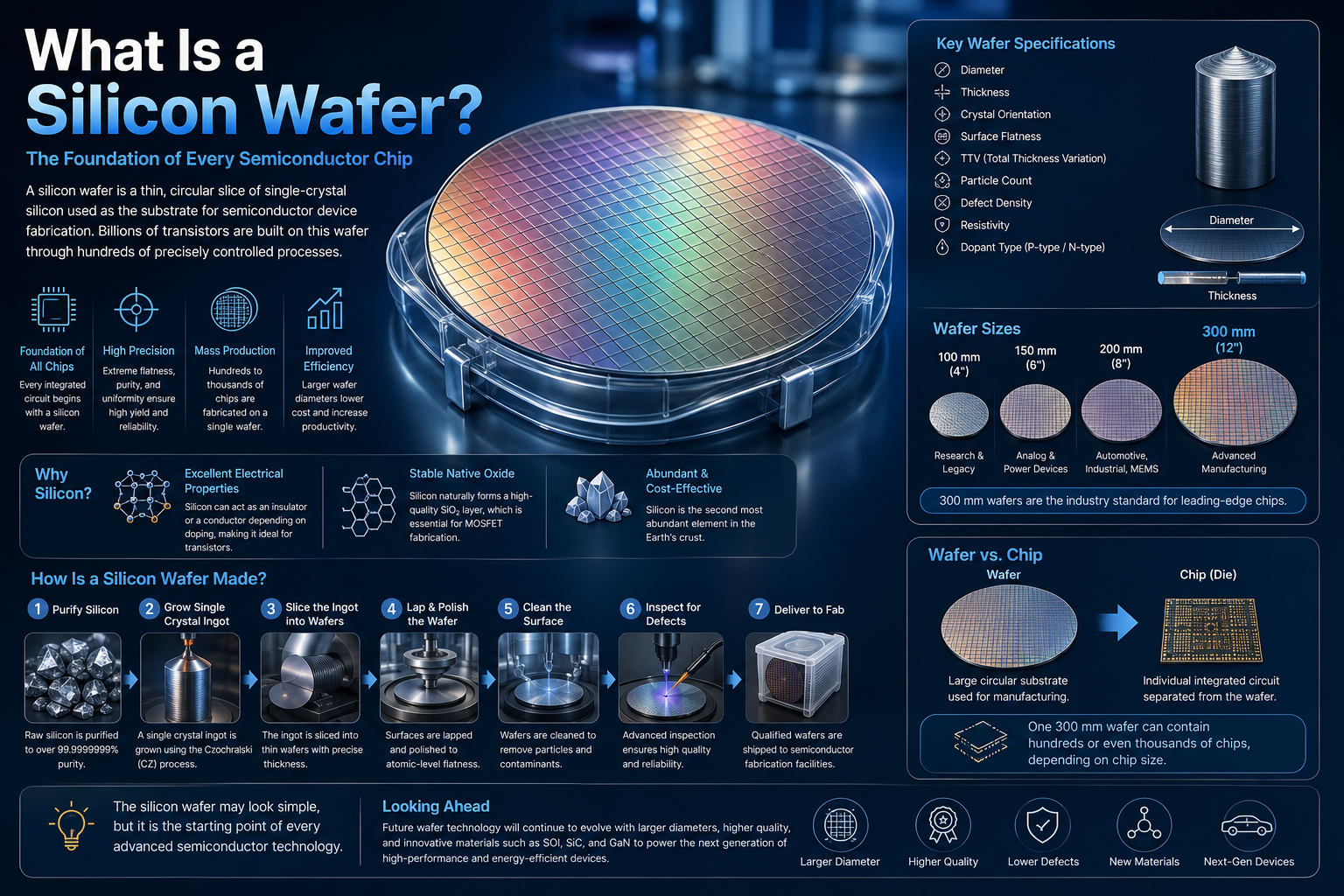
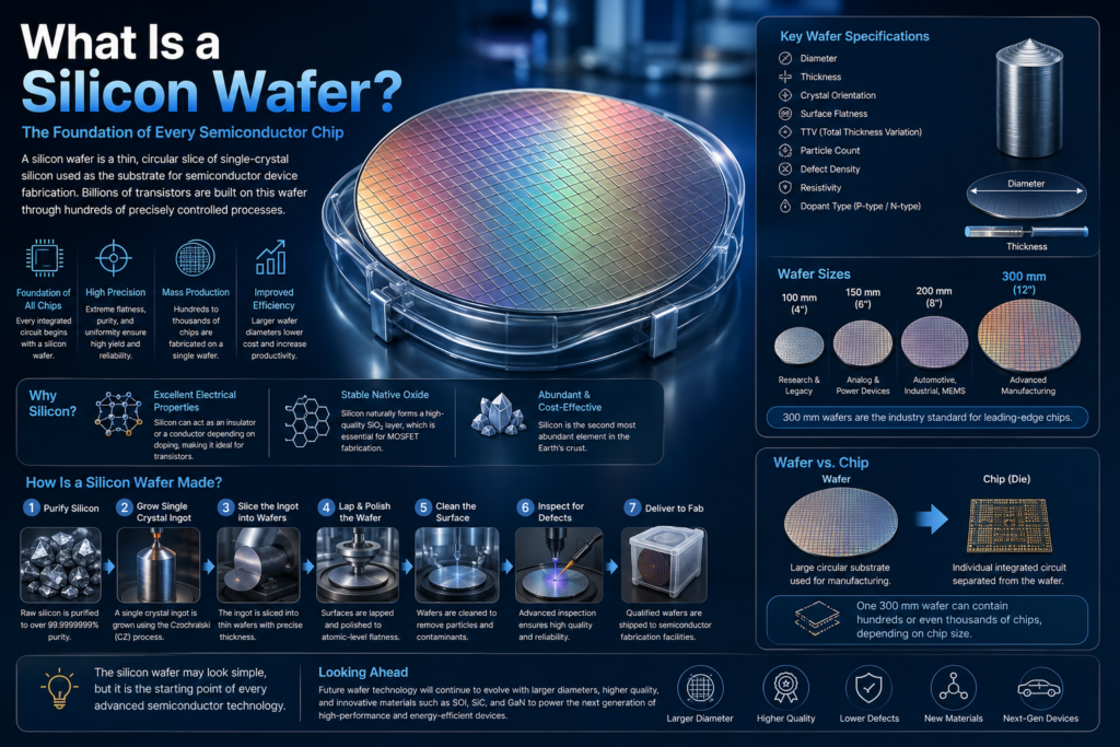
A silicon wafer is a thin, circular substrate made primarily from single-crystal silicon.
It serves as the base material on which integrated circuits are fabricated.
Rather than manufacturing one chip at a time, semiconductor companies build hundreds or thousands of identical chips simultaneously across the surface of a single wafer.
After fabrication and electrical testing are complete, the wafer is cut into individual rectangular pieces called dies. Each functional die can then be packaged as a semiconductor chip.
A concise definition, specification summary, and related terminology can later be provided through the dedicated Silicon Wafer entry in the iAtlas Library.
This Semiconductor article focuses instead on why silicon wafers became the dominant platform for modern chip manufacturing.
Why Is Silicon Used for Semiconductor Wafers?
Silicon became the foundation of the semiconductor industry because it offers a practical combination of electrical performance, material stability, manufacturability, and cost efficiency.
1. Controllable Electrical Properties
Pure silicon is a semiconductor, meaning its electrical conductivity lies between that of a conductor and an insulator.
Its electrical behavior can be precisely modified by introducing small amounts of dopant atoms.
This makes it possible to create:
- P-type regions
- N-type regions
- Transistor channels
- Source and drain structures
- Diodes and junctions
The ability to control conductivity makes silicon highly suitable for integrated circuit manufacturing.
2. A Stable Native Oxide
One of silicon’s most important advantages is its ability to form a high-quality oxide layer known as silicon dioxide, or SiO₂.
Silicon dioxide can act as:
- An electrical insulator
- A surface protection layer
- A masking layer
- A dielectric material
- A process barrier
The relationship between silicon and silicon dioxide played a major role in the development of MOSFET technology and modern integrated circuits.
Many other semiconductor materials do not form an oxide layer with the same level of stability and process compatibility.
3. Abundant Raw Material
Silicon is one of the most abundant elements in the Earth’s crust.
Although semiconductor-grade silicon requires extensive purification, the raw material itself is widely available.
This abundance helped make silicon more economical for mass production than many alternative semiconductor materials.
4. Mechanical and Thermal Stability
Silicon wafers can withstand many demanding manufacturing conditions.
During fabrication, wafers may experience:
- High temperatures
- Plasma exposure
- Chemical cleaning
- Vacuum processing
- Mechanical polishing
- Repeated handling by automated equipment
Silicon provides the mechanical strength and thermal stability required to survive these processes while maintaining dimensional accuracy.
5. A Mature Manufacturing Ecosystem
The semiconductor industry has spent decades developing equipment, chemicals, process recipes, inspection systems, and factories optimized for silicon wafers.
This mature ecosystem includes:
- Crystal growers
- Wafer manufacturers
- Lithography systems
- Etching equipment
- Deposition tools
- Cleaning systems
- Inspection equipment
- Automated wafer handling systems
Because so much of the global semiconductor infrastructure is built around silicon, replacing it entirely would require enormous technical and economic changes.
How Silicon Wafers Are Manufactured
Producing a semiconductor-grade wafer requires much more than cutting a piece of silicon into a circular shape.
The general manufacturing flow includes:
- Purification of raw silicon
- Growth of a single-crystal ingot
- Ingot shaping and diameter control
- Wafer slicing
- Edge grinding
- Lapping
- Chemical treatment
- Polishing
- Cleaning
- Inspection and grading
Each stage is designed to produce a wafer with extremely high purity, low defect density, precise dimensions, and exceptional surface flatness.
From Raw Silicon to Single-Crystal Ingot
The process begins with silicon that has been purified to an extremely high level.
This purified material is melted inside a controlled environment.
A small seed crystal is then introduced into the molten silicon and slowly pulled upward while rotating.
As the silicon cools around the seed, it forms a large cylindrical single crystal called an ingot.
This method is widely known as the Czochralski process, or CZ process.
The crystal orientation, diameter, dopant concentration, and defect level of the ingot must be carefully controlled because these properties will later affect every wafer cut from it.
➡️ Continue reading: How the Czochralski Process Creates Single-Crystal Silicon
From Ingot to Wafer
Once the ingot has been grown, it is prepared for slicing.
The cylindrical crystal is shaped to the required diameter and then cut into thin discs using precision wire-saw equipment.
However, freshly sliced wafers are not yet suitable for semiconductor manufacturing.
Their surfaces may contain:
- Saw marks
- Mechanical damage
- Thickness variation
- Surface contamination
- Edge defects
The wafers therefore undergo additional processing, including lapping, chemical etching, polishing, and cleaning.
The final goal is to create an ultra-flat, mirror-like surface suitable for nanometer-scale patterning.
Why Surface Flatness Is Critical
Modern semiconductor structures are built through many repeated process layers.
If the wafer surface is uneven, later processes may suffer from:
- Lithography focus errors
- Non-uniform film deposition
- Inconsistent etching
- Overlay problems
- Poor electrical performance
As device dimensions become smaller, even minor surface variation becomes increasingly important.
This is why parameters such as wafer bow, warp, thickness variation, and local flatness are carefully measured.
A high-quality wafer provides a stable foundation for accurate pattern transfer across the entire surface.
Wafer Sizes and Manufacturing Productivity
Semiconductor wafer diameters have increased over time as the industry has pursued higher productivity.
Common wafer sizes include:
| Wafer diameter | Common applications |
|---|---|
| 100 mm | Research, specialty devices, legacy production |
| 150 mm | Analog, sensor, and power applications |
| 200 mm | Automotive, industrial, MEMS, analog, power devices |
| 300 mm | Advanced logic, memory, AI, and high-volume manufacturing |
Today, 300 mm wafers are widely used in advanced semiconductor manufacturing.
The main advantage of a larger wafer is that more chips can be fabricated during a single production cycle.
Because many process steps are performed on the whole wafer, increasing the number of dies per wafer can improve equipment productivity and reduce manufacturing cost per chip.
Why the Industry Uses 300 mm Wafers
A 300 mm wafer has significantly more usable surface area than a 200 mm wafer.
This allows semiconductor manufacturers to produce more dies per batch while using many of the same core process steps.
The benefits include:
- More chips per wafer
- Higher equipment productivity
- Lower processing cost per die
- Better suitability for high-volume manufacturing
- Improved automation efficiency
However, larger wafers also create technical challenges.
They require:
- More precise handling
- Greater equipment uniformity
- Improved temperature control
- Better deposition and etching consistency
- More advanced defect inspection
The shift to 300 mm production therefore required major changes across the semiconductor equipment and materials ecosystem.
Wafer Size Does Not Determine Chip Size
A larger wafer does not necessarily mean that each semiconductor chip is larger.
Wafer diameter and die size are separate concepts.
A large wafer may contain:
- Many small chips
- Fewer large chips
- A mixture of test structures and production dies
The number of usable chips depends on factors such as:
- Individual die area
- Edge exclusion
- Process defect density
- Circuit design
- Wafer yield
Large AI processors may occupy significantly more wafer area than small power-management or sensor chips.
As a result, the same 300 mm wafer can produce very different numbers of finished dies depending on the product.
Crystal Orientation
Silicon wafers are produced with specific crystal orientations.
The most commonly discussed orientations include:
- (100)
- (111)
- (110)
Crystal orientation influences how the material behaves during processes such as oxidation, etching, and device fabrication.
The (100) orientation is widely used for CMOS integrated circuits because it offers favorable electrical and interface characteristics.
Other orientations may be selected for MEMS, sensors, power devices, or specialized semiconductor structures.
P-Type and N-Type Wafers
Silicon wafers can be manufactured as either P-type or N-type substrates.
P-Type Wafer
A P-type wafer is typically created by adding acceptor dopants that increase the concentration of holes.
N-Type Wafer
An N-type wafer is created using donor dopants that increase the concentration of free electrons.
The choice between P-type and N-type depends on:
- Device architecture
- Electrical design
- Manufacturing process
- Performance requirements
- Reliability targets
Dopant concentration also affects wafer resistivity, which is an important electrical specification.
Key Silicon Wafer Specifications
Semiconductor manufacturers evaluate wafers using a wide range of physical, electrical, and surface-quality parameters.
Important specifications include:
- Diameter
- Thickness
- Crystal orientation
- Dopant type
- Resistivity
- Total Thickness Variation
- Surface flatness
- Bow
- Warp
- Particle count
- Surface roughness
- Crystal defect density
- Edge profile
- Oxygen concentration
- Carbon concentration
These values are selected according to the manufacturing process and device being produced.
A wafer intended for advanced logic may require different characteristics from a wafer used for analog, MEMS, automotive, or power applications.
Total Thickness Variation
Total Thickness Variation, commonly called TTV, describes the difference between the thickest and thinnest points across a wafer.
Low TTV is important because semiconductor processes assume that the wafer surface remains highly uniform.
Excessive thickness variation can affect:
- Lithography focus
- Chuck contact
- Process uniformity
- Film thickness
- Wafer handling
As semiconductor dimensions shrink, tighter thickness control becomes increasingly important.
Bow and Warp
A wafer may not remain perfectly flat when it is unsupported.
Two common measurements used to describe wafer shape are bow and warp.
Bow
Bow describes the overall curvature of the wafer relative to a reference plane.
Warp
Warp describes the total variation in wafer shape across the entire surface.
Excessive bow or warp may create problems during lithography, bonding, inspection, and automated transfer.
These parameters become especially important when wafers include complex film stacks or undergo high-temperature processing.
Why Wafer Quality Affects Yield
Manufacturing yield refers to the percentage of dies that function correctly after fabrication.
Wafer quality can influence yield from the very beginning of the process.
Defects in the substrate may cause:
- Electrical leakage
- Crystal-related failure
- Pattern distortion
- Film non-uniformity
- Local process instability
- Die rejection
A defect that appears insignificant at the wafer stage may create a critical failure after hundreds of process steps have been completed.
For this reason, semiconductor manufacturers carefully inspect incoming wafers before they enter production.
Higher-quality wafers may cost more initially, but they can reduce the much larger cost associated with losing completed dies later in the process.
Wafer Handling and Contamination Control
Silicon wafers must remain extremely clean throughout manufacturing.
Particles, metals, moisture, organic residue, and chemical contamination can interfere with device fabrication.
Wafers are therefore handled using:
- Automated robots
- Vacuum end effectors
- Edge-grip systems
- Wafer carriers
- FOUPs
- Controlled cleanroom environments
Direct human contact with the wafer surface is avoided.
Specialized research and development processes may also require inert handling environments to protect air-sensitive materials or interfaces.
Silicon Wafer vs. Semiconductor Chip
A silicon wafer and a semiconductor chip are not the same thing.
Silicon Wafer
A wafer is the circular substrate used during semiconductor manufacturing.
It may contain hundreds or thousands of repeated circuit patterns.
Die
A die is one individual integrated circuit separated from the completed wafer.
Packaged Chip
A packaged chip is a tested die placed inside a protective package with electrical connections to the outside system.
The overall sequence can be summarized as:
Silicon wafer → Fabricated wafer → Individual die → Packaged semiconductor chip
Understanding this difference makes the overall semiconductor manufacturing flow much easier to follow.
Silicon Is Important, but It Is Not the Only Wafer Material
Silicon dominates conventional integrated circuit manufacturing, but other materials are increasingly important for specialized applications.
Silicon-on-Insulator
Silicon-on-Insulator, or SOI, uses a thin silicon layer separated from the bulk substrate by an insulating layer.
SOI wafers can support improved electrical isolation, lower parasitic capacitance, and specialized device architectures.
Silicon Carbide
Silicon carbide, or SiC, is widely used for high-voltage and high-temperature power semiconductor applications.
It is especially important in:
- Electric vehicles
- Charging systems
- Renewable energy
- Industrial power conversion
Gallium Nitride
Gallium nitride, or GaN, is used in high-frequency and high-efficiency power applications.
GaN devices can be produced using different substrate approaches depending on the technology and application.
These materials do not eliminate the importance of silicon. Instead, they expand the range of semiconductor platforms available for specific performance requirements.
The Future of Silicon Wafers
Silicon wafers will remain central to the semiconductor industry, but wafer technology will continue to evolve.
Key development areas include:
- Lower crystal defect density
- Improved surface flatness
- Better edge control
- Higher-purity materials
- Engineered substrates
- SOI wafer development
- Wafer bonding
- Thinner wafers
- Backside power delivery
- 3D integration
- Advanced packaging applications
As semiconductor devices become more complex, the wafer must support not only front-end transistor manufacturing but also increasingly demanding bonding, stacking, and packaging processes.
The future of chip manufacturing therefore depends not only on smaller transistors, but also on more advanced wafer engineering.
Key Takeaways
- Silicon wafers provide the physical foundation for modern semiconductor manufacturing.
- Silicon became dominant because of its controllable electrical properties, stable oxide, material availability, and mature manufacturing ecosystem.
- Wafer purity, flatness, resistivity, crystal orientation, and defect density directly influence semiconductor yield.
- Larger wafers improve manufacturing productivity by enabling more chips to be processed at once.
- 300 mm wafers are widely used for advanced logic, memory, AI, and high-volume semiconductor production.
- Alternative substrates such as SOI, SiC, and GaN complement silicon in specialized applications.
- As semiconductor devices evolve, wafer engineering will become increasingly important for 3D integration and advanced packaging.
📖 Semiconductor Learning Path
Previous: 💻 Semiconductor #1 | What Is Semiconductor Manufacturing?
Current: 💻 Semiconductor #2 | Why Silicon Wafers Are the Foundation of Modern Chips
Next: 💻 Semiconductor #3 | How the Czochralski Process Creates Single-Crystal Silicon
📚 Continue Reading
- 💻 Semiconductor #1 | What Is Semiconductor Manufacturing?
- 💻 Semiconductor #3 | How the Czochralski Process Creates Single-Crystal Silicon
- 💻 Semiconductor #4 | How Silicon Ingots Become Semiconductor Wafers
- 💻 Semiconductor #5 | How Photolithography Creates Microscopic Circuit Patterns
- 💻 Semiconductor #6 | How Plasma Etching Shapes Modern Semiconductor Devices
References
🔷 About iAtlas
iAtlas is an independent publication covering batteries, semiconductors, OLED, advanced materials, AI, and global industrial trends.
We transform complex industrial developments into clear, reliable, and easy-to-understand insights.
Whether you’re following today’s industry news or building long-term expertise, iAtlas helps you understand not only what happened, but why it matters.
Technology creates change.
Insight creates opportunity.
— iAtlas