How Thin Film Deposition Builds Semiconductor Devices Layer by Layer
💻 iAtlas Semiconductor #7 | 📘 Manufacturing → Deposition
Introduction
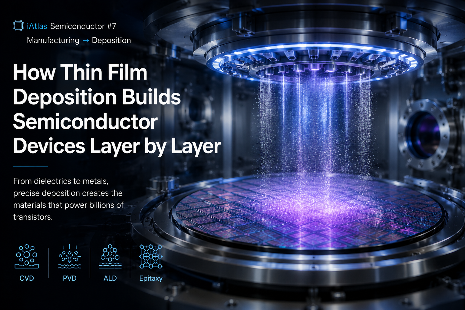
Thin film deposition builds the microscopic material layers that form modern semiconductor devices.
A semiconductor chip is not made by simply carving circuits into a silicon wafer. Instead, manufacturers repeatedly add, pattern, remove, and modify extremely thin layers of materials to create transistors, insulating structures, contacts, and metal interconnects.
Some of these films are only a few nanometers thick.
Yet their thickness, composition, uniformity, and interface quality can directly influence how billions of transistors operate.
This is why thin film deposition is one of the fundamental technologies behind semiconductor manufacturing.
From dielectric layers and metal conductors to advanced gate materials, deposition allows engineers to construct semiconductor devices layer by layer.
Why Thin Film Deposition Matters
Modern semiconductor devices contain many different materials stacked vertically and patterned across a silicon wafer.
Each material performs a specific function.
A deposited film may act as:
- An electrical conductor
- An insulating dielectric
- A diffusion barrier
- A hard mask
- A gate material
- An adhesion layer
- A protective layer
- A semiconductor layer
The challenge is not simply depositing material.
Manufacturers must control the film at extremely small dimensions while maintaining consistent properties across an entire wafer.
Important parameters include:
- Film thickness
- Thickness uniformity
- Chemical composition
- Conformality
- Step coverage
- Film stress
- Electrical properties
- Interface quality
- Defect density
As semiconductor structures become smaller and increasingly three-dimensional, controlling these properties becomes even more important.
Where Deposition Fits in Semiconductor Manufacturing
Semiconductor fabrication is a repetitive sequence of material formation and pattern transfer.
A simplified cycle might look like:
Deposition → Photoresist → Photolithography → Etching → Cleaning → Deposition
Thin film deposition first creates a material layer.
Photolithography then defines the desired pattern.
Plasma etching removes selected portions of that layer.
Another material can then be deposited, patterned, and etched.
This cycle may occur many times during fabrication.
The result is a complex three-dimensional semiconductor structure constructed through repeated material addition and removal.
What Is Thin Film Deposition?
Thin film deposition is the controlled formation of extremely thin material layers on the surface of a substrate, typically a semiconductor wafer.
Film thickness can range from several micrometers down to only a few nanometers—or even approach atomic-scale control in advanced processes.
Several deposition technologies are used because no single method can satisfy every semiconductor application.
The major approaches include:
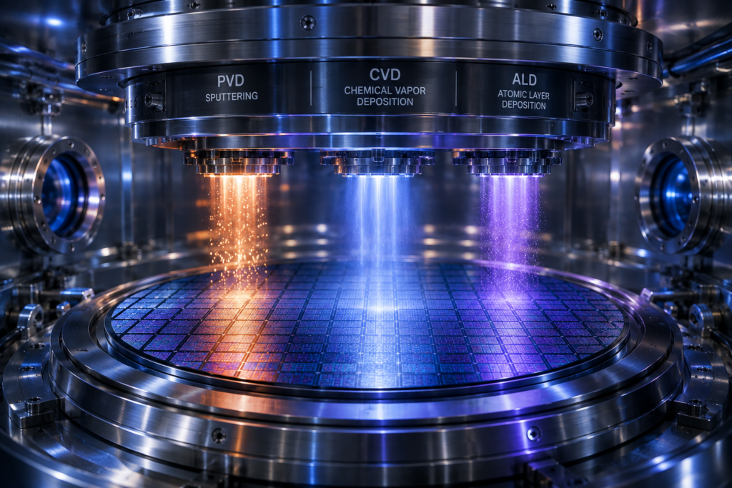
- Chemical Vapor Deposition (CVD)
- Physical Vapor Deposition (PVD)
- Atomic Layer Deposition (ALD)
- Epitaxial Growth
Each uses a different mechanism to form material on the wafer.
Chemical Vapor Deposition (CVD)
Chemical Vapor Deposition, or CVD, forms thin films through chemical reactions involving gaseous precursor materials.
Process gases enter a controlled reaction chamber and reach the wafer surface.
Under appropriate temperature and pressure conditions, chemical reactions occur and create a solid film.
Unwanted gaseous reaction products are then removed from the chamber.
A simplified concept is:
Gaseous Precursors → Surface Reaction → Solid Thin Film + Gaseous By-products
CVD can deposit many materials used in semiconductor manufacturing, including dielectric and semiconductor films.
Why CVD Is Widely Used
CVD offers several important advantages:
- Good film uniformity
- Relatively high deposition rates
- Ability to process complex structures
- Wide range of available materials
- Good wafer-scale productivity
Different forms of CVD are used depending on the application.
These include:
LPCVD
Low Pressure Chemical Vapor Deposition operates at reduced pressure and is commonly used when high-quality, uniform films are required.
PECVD
Plasma Enhanced Chemical Vapor Deposition uses plasma energy to promote chemical reactions.
This allows deposition at lower temperatures than many conventional thermal CVD processes.
Lower processing temperatures can be important when previously fabricated structures cannot tolerate high thermal exposure.
Physical Vapor Deposition (PVD)
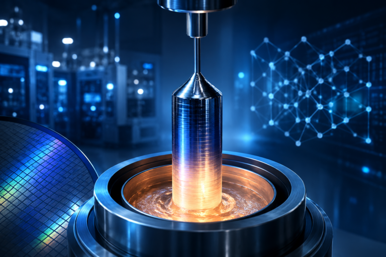
Physical Vapor Deposition, or PVD, forms a thin film by physically transferring material from a solid source to the wafer.
One of the most important semiconductor PVD technologies is sputtering.
In a sputtering process, energetic ions bombard a target material.
Atoms are ejected from the target and travel through the vacuum chamber before depositing onto the wafer.
The simplified process is:
Target → Ion Bombardment → Ejected Atoms → Wafer → Thin Film
PVD is widely associated with metallic and conductive films.
Why Vacuum Matters in PVD
PVD processes typically operate under vacuum.
Lower pressure allows deposited atoms to travel through the chamber with fewer unwanted collisions.
Vacuum also helps engineers control:
- Gas composition
- Contamination
- Particle transport
- Deposition rate
- Film properties
Because semiconductor films are extremely sensitive to impurities, stable vacuum conditions are critical for repeatable PVD performance.
Atomic Layer Deposition (ALD)
As semiconductor structures became smaller and more three-dimensional, conventional deposition methods faced new challenges.
One of the most important solutions is Atomic Layer Deposition, or ALD.
ALD forms films through a sequence of self-limiting surface reactions.
Instead of continuously supplying all reactants at once, precursor gases are introduced separately.
A simplified ALD cycle is:
Precursor A → Purge → Precursor B → Purge → Repeat
Each cycle deposits a very small amount of material.
Repeating the cycle gradually builds the required film thickness.
Why ALD Is Important for Advanced Chips
The major strength of ALD is extremely precise thickness control combined with excellent conformality.
Imagine coating a flat surface.
Many deposition methods can do this effectively.
Now imagine coating the inside of a deep nanoscale trench or wrapping a uniform layer around a complex three-dimensional transistor structure.
This is much more difficult.
ALD is particularly valuable because it can form highly uniform films over complex surface geometries.
This capability is increasingly important for:
- FinFET structures
- Gate-All-Around (GAA) transistors
- 3D NAND
- Advanced capacitors
- High-k dielectrics
- Barrier layers
As semiconductor architecture moves further into three dimensions, ALD becomes increasingly important.
What Is Conformality?
Conformality describes how uniformly a deposited film covers different parts of a three-dimensional structure.
Consider a deep trench.
An ideal conformal film has approximately the same thickness:
- At the top
- Along the sidewalls
- At the bottom
Poor conformality may leave some regions too thick and others too thin.
For planar semiconductor devices this was less challenging.
For modern 3D structures, however, conformal deposition is critical.
This is one reason ALD has become such an important technology for advanced semiconductor manufacturing.
CVD vs. PVD vs. ALD
The major deposition technologies have different strengths.
| Characteristic | CVD | PVD | ALD |
|---|---|---|---|
| Basic mechanism | Chemical reaction | Physical material transfer | Sequential surface reaction |
| Deposition rate | Relatively high | Relatively high | Relatively slow |
| Thickness control | Good | Good | Excellent |
| Conformality | Good | Limited for complex structures | Excellent |
| Complex 3D structures | Good | More challenging | Excellent |
| Typical strength | Versatility | Metal films | Atomic-scale control |
These technologies are not simply competitors.
A modern semiconductor fab uses different deposition methods for different materials and structures.
Epitaxial Growth
Another important semiconductor deposition technology is epitaxy.
Epitaxial growth creates a crystalline semiconductor layer whose crystal structure follows the underlying substrate.
Unlike many deposited films, which may be amorphous or polycrystalline, epitaxial layers maintain controlled crystal orientation.
Epitaxy can be used to engineer semiconductor regions with specific:
- Electrical properties
- Composition
- Doping
- Thickness
- Crystal characteristics
This makes epitaxial growth important for advanced transistor structures and specialized semiconductor devices.
Thin Films in a Modern Transistor
To understand the importance of deposition, consider a modern transistor.
It may contain multiple precisely engineered materials, including:
- Silicon or silicon-germanium channels
- High-k gate dielectrics
- Metal gate materials
- Spacer materials
- Contact metals
- Barrier layers
- Interlayer dielectrics
Each material may require a different deposition technology.
The final transistor therefore represents not one deposition process, but a carefully controlled sequence of many deposition steps.
High-k Dielectric Deposition
As transistors became smaller, traditional silicon dioxide gate dielectrics became increasingly difficult to scale.
The semiconductor industry therefore introduced high-k dielectric materials.
These materials provide higher dielectric constants while allowing a physically thicker layer than an equivalent silicon dioxide dielectric.
Materials such as hafnium-based dielectrics can require highly precise deposition.
ALD is particularly useful because it provides fine thickness control and excellent coverage over advanced device structures.
Deposition and Gate-All-Around Transistors
Gate-All-Around transistors illustrate why deposition technology has become increasingly sophisticated.
In a GAA architecture, gate material surrounds nanoscale semiconductor channels.
Creating these structures requires films to coat extremely small three-dimensional surfaces with exceptional uniformity.
Processes may require precise deposition of:
- Dielectric layers
- Work-function metals
- Barrier materials
- Semiconductor layers
Small thickness variations can change electrical behavior.
As a result, advanced deposition has become one of the enabling technologies for GAA transistor scaling.
Thin Film Deposition in 3D NAND
3D NAND presents a different challenge.
Instead of shrinking everything horizontally, memory cells are stacked vertically.
Modern devices may contain hundreds of layers.
Manufacturing these structures requires repeated deposition of extremely uniform films across large vertical stacks.
Important requirements include:
- Thickness consistency
- Low defect density
- Film stress control
- Uniform composition
- High productivity
As NAND layer counts increase, deposition equipment must process increasingly complex structures without sacrificing uniformity.
Film Stress and Why It Matters
A thin film may appear perfectly flat while still containing internal mechanical stress.
This stress can develop because of:
- Deposition conditions
- Thermal expansion differences
- Film composition
- Crystal structure
Excessive film stress can cause:
- Wafer bow
- Cracking
- Delamination
- Pattern distortion
- Reliability problems
Controlling film stress is therefore an important part of deposition process engineering.
Temperature Control
Temperature affects chemical reactions, film growth, surface mobility, and material properties.
However, semiconductor manufacturers cannot always use higher temperatures to improve film quality.
Once sensitive device structures have been created, excessive heat may damage previously formed layers or alter dopant distributions.
This creates a concept known as the thermal budget.
Advanced deposition technologies must therefore achieve the desired film quality while staying within increasingly strict temperature limits.
Deposition Uniformity Across the Wafer
Modern semiconductor production primarily uses 300 mm wafers for advanced manufacturing.
A deposition process must produce nearly identical film characteristics from the center of the wafer to the edge.
Even small differences can change:
- Electrical resistance
- Etch behavior
- Critical dimensions
- Device performance
Uniformity must also remain consistent from wafer to wafer across high-volume production.
This requires precise control of:
- Gas flow
- Pressure
- Temperature
- Plasma conditions
- Precursor delivery
- Chamber condition
Why Chamber Condition Matters
The deposition chamber itself changes during operation.
Materials can gradually accumulate on internal chamber surfaces.
These deposits may influence process conditions or become sources of particles.
Semiconductor equipment therefore relies on carefully controlled:
- Chamber cleaning
- Preventive maintenance
- Process seasoning
- Gas delivery
- Vacuum performance
- Temperature management
Consistent thin films require not only accurate recipes but also a stable process environment.
Deposition and Etching Work Together
Deposition and etching are closely connected.
Deposition adds material.
Etching removes selected material.
Photolithography determines where that removal should occur.
Together, these technologies create the fundamental manufacturing cycle:
Deposit → Pattern → Etch → Repeat
Modern semiconductor fabrication can therefore be understood as an extraordinarily precise process of repeatedly building and sculpting materials at microscopic scales.
The Future of Thin Film Deposition
Thin film deposition is becoming increasingly important as semiconductor scaling moves from primarily two-dimensional shrinking toward three-dimensional structural engineering.
Future development areas include:
- Atomic-scale thickness control
- More selective deposition
- Area-selective ALD
- New high-k materials
- New metal interconnect materials
- Lower-temperature processing
- Improved precursor chemistry
- Better conformality
- Advanced GAA deposition
- High-aspect-ratio 3D memory processes
The future of semiconductor scaling will depend not only on how small patterns can be printed, but also on how precisely materials can be placed where they are needed.
Key Takeaways
- Thin film deposition creates the material layers used to build semiconductor devices.
- Modern chips require conductive, dielectric, barrier, semiconductor, and other functional films.
- CVD forms films through chemical reactions involving gaseous precursors.
- PVD physically transfers material from a source to the wafer and is widely used for metal films.
- ALD uses sequential surface reactions to provide extremely precise thickness control and excellent conformality.
- Epitaxy creates crystalline semiconductor layers aligned with the underlying substrate.
- Advanced structures such as GAA transistors and 3D NAND are increasing the importance of conformal and atomic-scale deposition.
- Deposition, photolithography, and etching work together to build semiconductor devices layer by layer.
Frequently Asked Questions
What is thin film deposition in semiconductor manufacturing?
Thin film deposition is the controlled formation of extremely thin material layers on a semiconductor wafer. These films can serve as conductors, insulators, barriers, masks, or active semiconductor layers.
What is the difference between CVD and PVD?
CVD forms films through chemical reactions involving gaseous precursors, while PVD physically transfers material from a solid source to the wafer.
Why is ALD important in advanced semiconductor manufacturing?
ALD provides extremely precise thickness control and excellent conformality, making it well suited to complex three-dimensional structures such as GAA transistors and 3D NAND.
What does conformal deposition mean?
Conformal deposition means that a film maintains relatively uniform thickness across the top, sidewalls, and recessed surfaces of a three-dimensional structure.
Why are multiple deposition technologies needed?
Different semiconductor materials and structures require different combinations of temperature, film quality, deposition rate, conformality, and material compatibility. No single deposition technology is optimal for every application.
📖 Semiconductor Learning Path
Previous: 💻 Semiconductor #6 | How Plasma Etching Shapes Semiconductor Devices
⬇️
Current: 💻 Semiconductor #7 | How Thin Film Deposition Builds Semiconductor Devices Layer by Layer
⬇️
Next: 💻 Semiconductor #8 | How Ion Implantation Engineers Silicon at the Atomic Level
📚 Continue Reading
- 💻 Semiconductor #5 | How Photolithography Creates Billions of Transistors
- 💻 Semiconductor #6 | How Plasma Etching Shapes Semiconductor Devices
- 💻 Semiconductor #8 | How Ion Implantation Engineers Silicon at the Atomic Level
- 💻 Semiconductor #9 | How CMP Creates an Ultra-Flat Semiconductor Surface
- 💻 Semiconductor #10 | How Semiconductor Inspection & Metrology Find Nanometer-Scale Defects
References
Recommended primary sources for this article:
🔷 About iAtlas
iAtlas is an independent publication covering batteries, semiconductors, OLED, advanced materials, AI, and global industrial trends.
We transform complex industrial developments into clear, reliable, and easy-to-understand insights.
Whether you’re following today’s industry news or building long-term expertise, iAtlas helps you understand not only what happened, but why it matters.
Technology creates change.
Insight creates opportunity.
— iAtlas