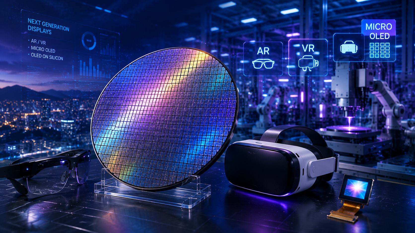
Why 300mm Wafers Matter for AR/VR
The Manufacturing Shift Behind the Next Generation of Displays
📰 iAtlas Daily #3 | July 4, 2026
Today’s Highlights
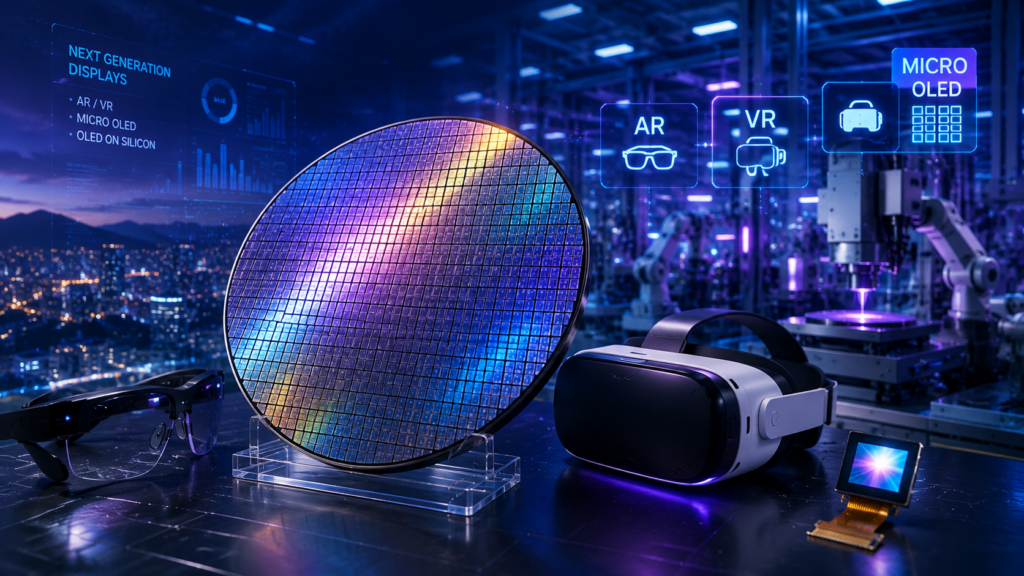
- The AR and VR industry is accelerating the transition from 200mm to 300mm silicon wafer production.
- Larger wafers improve manufacturing efficiency while enabling scalable Micro OLED production.
- Higher production capacity also increases the importance of high-purity materials and precision manufacturing.
Cover Story
Why 300mm Wafers Matter
For decades, 200mm silicon wafers have been the standard platform for manufacturing OLED-on-Silicon (OLEDoS) displays.
Today, the industry is beginning a significant transition toward 300mm wafer platforms.
This shift is not simply about increasing wafer size.
It is about improving manufacturing efficiency, increasing production yield, and preparing for the mass production of next-generation AR and VR displays.
As devices become lighter, smaller, and capable of displaying higher resolutions, manufacturers require production technologies that can deliver both precision and scalability.
The transition to 300mm wafers is becoming one of the most important manufacturing trends in the display industry.
OLED
The Future of Micro OLED
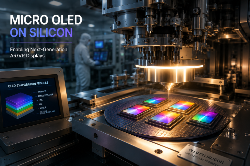
Unlike conventional OLED panels produced on glass substrates,
Micro OLED displays are fabricated directly on silicon wafers.
This enables several important advantages:
- Ultra-high pixel density
- Faster response times
- Lower power consumption
- Smaller display modules
These characteristics make Micro OLED one of the leading technologies for:
- AR Glasses
- VR Headsets
- Military optics
- Medical imaging systems
As demand for these applications grows, manufacturers are increasingly investing in 300mm production capabilities.
Semiconductor
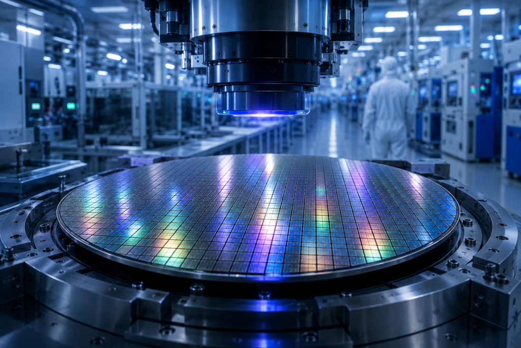
Bigger Wafers, Better Productivity
Moving from 200mm to 300mm wafers significantly increases manufacturing efficiency.
A larger wafer allows more display chips to be fabricated during each production cycle, reducing manufacturing cost per device.
Key advantages include:
- Higher throughput
- Better economies of scale
- Improved production yield
- Greater manufacturing capacity
Although larger wafers require tighter process control, the long-term benefits make the transition attractive for high-volume manufacturing.
Materials
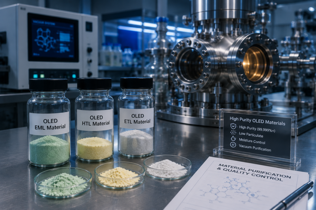
Manufacturing Quality Starts with Materials
As wafer size increases, manufacturing quality becomes even more important.
A small particle or impurity that affects a 200mm wafer becomes an even greater concern on a 300mm platform.
This is driving increased investment in:
- High-purity OLED materials
- Material purification technologies
- Vacuum sublimation processes
- Precision process control
Future manufacturing competitiveness will depend not only on equipment, but also on the quality of the materials entering the production line.
🎯 Atlas Radar
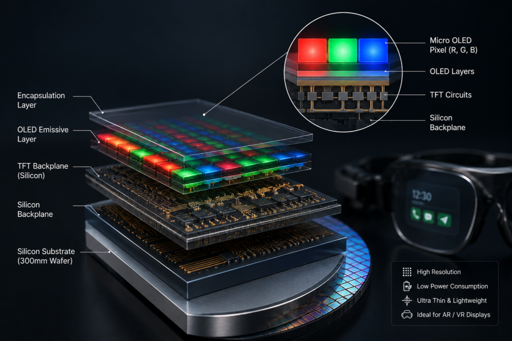
OLED on Silicon (OLEDoS)
OLEDoS combines OLED display technology with semiconductor manufacturing.
Instead of depositing OLED materials onto glass,
the organic layers are deposited directly onto silicon wafers.
Why It Matters
OLEDoS enables extremely high-resolution displays in compact form factors.
This technology is expected to play a key role in the future of AR, VR, mixed reality, and wearable devices.
🔭 Atlas Outlook
Looking Ahead
300mm Manufacturing Will Continue Expanding
As demand for AR and VR devices increases, manufacturers will continue investing in larger production platforms.
Material Innovation Will Become a Competitive Advantage
High-purity materials and advanced purification technologies will become increasingly important for improving manufacturing yield.
Semiconductor and Display Industries Will Converge
The transition to 300mm demonstrates how display manufacturing is increasingly adopting semiconductor manufacturing philosophies.
The boundaries between the two industries will continue to blur.
💡 Atlas Insight
The story is not simply about larger wafers.
It is about building the manufacturing foundation for the next generation of immersive technologies.
Higher productivity.
Higher precision.
Higher purity.
These three trends are defining the future of Micro OLED manufacturing.
Understanding them today helps explain where tomorrow’s display industry is heading.
Today’s Keywords
300mm Silicon Wafer
The industry-standard wafer size used in advanced semiconductor manufacturing and increasingly adopted for next-generation Micro OLED production.
OLED on Silicon (OLEDoS)
A display technology that deposits OLED materials directly onto silicon wafers, enabling ultra-high-resolution microdisplays.
High-Purity Materials
Materials refined to extremely low impurity levels, essential for advanced semiconductor and OLED manufacturing.
About iAtlas
iAtlas is an independent industry publication covering batteries, semiconductors, OLED, advanced materials, and emerging technologies.
Our mission is simple:
To explain not only what is happening, but why it matters.
Technology creates change.
Insight creates opportunity.
— iAtlas
📚 Continue Reading
Previous Daily
➡️ Why Korea’s Chip Giants Are Investing at the Same Time
Discover how Samsung Electronics and SK hynix are preparing for the AI era through long-term investments in semiconductors, advanced packaging, and next-generation manufacturing.
Also Recommended
➡️ Why Samsung’s New Gwangju Investment Matters
Explore why Samsung’s latest investment represents more than a factory expansion—and how it reflects Korea’s AI-driven manufacturing transformation.
About iAtlas
iAtlas is an independent publication covering batteries, semiconductors, OLED, advanced materials, AI, and global industrial trends.
We transform complex industrial developments into clear, reliable, and easy-to-understand insights.
Whether you’re following today’s industry news or building long-term expertise, iAtlas helps you understand not only what happened, but why it matters.
Technology creates change.
Insight creates opportunity.
— iAtlas