
Semiconductor Equipment Market Outlook 2026
Why the AI Investment Cycle Is Expanding Beyond Chips
iAtlas | Insight | Market Outlook #10

The semiconductor equipment market outlook for 2026 shows that the AI investment cycle is expanding far beyond the chips themselves.
AI accelerators, HBM, advanced logic and increasingly complex semiconductor packages all require new manufacturing capacity.
But semiconductor capacity cannot be created simply by building a factory.
Every new fab requires hundreds of highly specialized manufacturing systems for:
Lithography
Deposition
Etching
Cleaning
Ion Implantation
Inspection
Metrology
Wafer Handling
Packaging
Testing
As semiconductor structures become smaller and more three-dimensional, the number and complexity of these process steps continue to increase.
SEMI forecasts global semiconductor manufacturing equipment sales to reach a record $165.9 billion in 2026, up 23.2% year over year.
The Wafer Fab Equipment segment alone is expected to reach approximately $143.9 billion, while strong AI demand is also pushing investment higher in semiconductor test and advanced packaging equipment.
AI is therefore creating more than a semiconductor-device boom.
It is creating a manufacturing-equipment investment cycle.
Key Takeaways
- Global semiconductor manufacturing equipment sales are forecast to reach approximately $165.9 billion in 2026, up 23.2% year over year.
- Wafer Fab Equipment sales are projected at approximately $143.9 billion, up 23.1%.
- Foundry and logic WFE sales are expected to reach approximately $78 billion, driven by AI accelerators, HPC and 2nm investment.
- Memory investment is accelerating as HBM, DDR5 and advanced NAND require new capacity and more complex processes.
- 300mm memory-equipment investment is projected to reach approximately $52 billion in 2026, including around $37 billion for DRAM.
- Semiconductor test-equipment sales are projected to rise 31% to $15.3 billion in 2026.
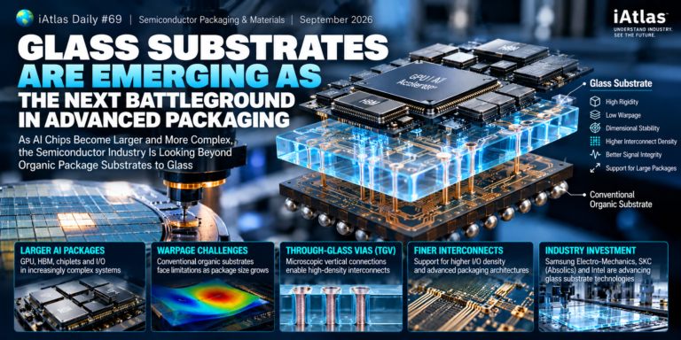
- Assembly and packaging equipment is expected to reach approximately $6.7 billion, supported by HBM, chiplets and heterogeneous integration.
- Global 300mm front-end fab equipment spending is now projected at approximately $149 billion in 2026, up 31% year over year in SEMI’s latest Q3 outlook.
- Semiconductor equipment demand is increasingly being driven by technology complexity, not only by wafer-capacity growth.
- AI investment is strengthening demand across lithography, deposition, etch, process control, packaging and test simultaneously.
1. Semiconductor Equipment Is Entering a New Growth Cycle
The semiconductor equipment industry has always been cyclical.
Chipmakers invest aggressively when demand is strong.
New fabs are constructed.
Capacity increases.
Eventually, investment slows as supply catches up with demand.
That cycle has not disappeared.
But the current expansion has an unusual characteristic:
multiple technology transitions are happening at the same time.
AI requires more leading-edge logic.
HBM requires more advanced DRAM.
3D NAND continues adding layers.
2nm introduces new transistor architectures.
Advanced packaging combines increasingly complex chiplets and memory stacks.
Each transition requires additional equipment.
That means equipment demand is being driven not only by:
More Capacity
but also by:
More Process Complexity
The two forces are now reinforcing each other.
2. 2026 Is Becoming a Record Equipment Year
SEMI’s mid-year forecast estimates global semiconductor manufacturing equipment sales of approximately $165.9 billion in 2026.
That represents growth of 23.2% compared with the previous year.
The organization expects the expansion to continue, with global equipment sales potentially reaching approximately $229.5 billion by 2028.
The largest component is Wafer Fab Equipment, or WFE.
WFE includes much of the equipment used before wafers are cut into individual chips, including:
- Lithography
- Deposition
- Etch
- Clean
- Process control
- Wafer processing infrastructure
SEMI expects WFE sales to reach approximately $143.9 billion in 2026.
This is important because WFE represents the physical infrastructure required to transform semiconductor designs into actual chips.
The AI investment cycle therefore translates directly into equipment demand.
3. AI Is Driving Foundry and Logic Investment
AI accelerators require some of the world’s most advanced semiconductor processes.
As discussed in Market Outlook #09, leading-edge manufacturing is rapidly moving toward 3nm and 2nm.
SEMI expects WFE sales for foundry and logic applications to reach approximately $78 billion in 2026, representing growth of 18.9% year over year.
The main drivers include:
- AI accelerators
- High-performance CPUs
- Custom AI ASICs
- Premium mobile processors
- 2nm gate-all-around manufacturing
The transition toward GAA transistor architectures is particularly important.
Smaller transistors are no longer achieved simply by shrinking existing structures.
Manufacturers increasingly require entirely new device architectures.
That creates demand for new:
Deposition
Etching
Metrology
and
Process-Control
technologies.
The move toward 2nm is therefore also an equipment-technology transition.
4. Lithography Remains One of the Most Critical Bottlenecks
Lithography defines semiconductor patterns on wafers.
As transistor dimensions shrink, the ability to print increasingly small and precise features becomes more difficult.
Extreme Ultraviolet, or EUV, lithography has become essential for the most advanced semiconductor nodes.
ASML sits at the center of this transition.
In Q3 2026, ASML reported approximately €11.7 billion in quarterly revenue, selling 113 new lithography systems during the quarter.
The company expects total 2026 net sales of approximately €44–45 billion.
The industry is also preparing for High-NA EUV, designed to support future advanced-node scaling.
ASML and TSMC announced additional collaboration in September 2026 around future photomask formats intended to improve High-NA EUV productivity and scalability.
This highlights a broader point.
As semiconductor nodes become more advanced, lithography infrastructure itself must continue evolving.
5. Deposition Is Becoming More Important as Chips Become 3D
Modern semiconductor manufacturing involves repeatedly adding extremely thin films onto a wafer.
This is called deposition.
As semiconductor devices become more three-dimensional, film thickness and uniformity become increasingly important.
Important deposition technologies include:
- CVD
- PVD
- ALD
- Epitaxy
The move toward GAA transistors, advanced DRAM and increasingly complex NAND architectures creates demand for more precise materials engineering.
Applied Materials reported record quarterly revenue of approximately $9.12 billion in its fiscal Q3 2026, up 25% year over year.
The company specifically highlighted strong investment in:
- Leading-edge foundry/logic
- DRAM
- Advanced packaging
as AI adoption drives semiconductor-manufacturing demand.
Applied also introduced new deposition technologies for advanced DRAM, HBM and next-generation logic during 2026.
The reason is straightforward:
More complex semiconductor structures require more precise material layers.
6. Etch Is Becoming Equally Critical
After material is deposited, unwanted material often needs to be removed.
This is the role of etching.
Semiconductor etching has become dramatically more difficult as structures become:
- Narrower
- Deeper
- More three-dimensional
- More material-sensitive
In advanced logic, etching helps form increasingly complex transistor structures.
In NAND, very deep vertical channels must be created through hundreds of material layers.
In HBM, advanced processing is required around TSV and other integration structures.
Lam Research is one of the major companies exposed to these trends.
For the quarter ended September 2026, Lam reported revenue of approximately $8.22 billion, up 22% from the prior quarter.
This illustrates how equipment companies exposed to advanced memory and logic are benefiting from the current investment cycle.
As semiconductor architectures become more three-dimensional, etch intensity can rise even without equivalent wafer-capacity growth.
7. HBM Is Creating a New Memory Equipment Cycle
HBM is one of the strongest equipment investment drivers in 2026.
As covered in Market Outlook #06, producing HBM requires advanced DRAM wafers plus additional manufacturing steps.
The basic chain looks like:
Advanced DRAM
↓
TSV Formation
↓
Wafer Thinning
↓
Stacking
↓
Bonding
↓
Advanced Packaging
This makes HBM far more manufacturing-intensive than conventional DRAM.
SEMI expects 300mm memory-equipment investment to rise approximately 29% to $52 billion in 2026.
Within that total:
DRAM: approximately $37 billion
3D NAND: approximately $14 billion
Strong HBM and DDR5 demand are major contributors.
HBM therefore creates demand across both front-end and back-end equipment.
8. Memory Investment Is About Technology Migration, Not Just Capacity
An important distinction needs to be made.
More memory-equipment spending does not always mean proportionally more wafer capacity.
Advanced memory processes consume more equipment and can reduce effective output during technology transitions.
For example:
Advanced DRAM
requires increasingly complex patterning and materials.
HBM
uses advanced DRAM capacity but adds additional process steps.
Higher-layer NAND
requires increasingly difficult deposition and etch processes.
SEMI notes that memory capacity growth remains moderated by increasing process complexity even as equipment spending rises sharply.
This means equipment intensity per wafer can increase.
For equipment companies, that can be extremely important.
The market can grow even without equivalent growth in total semiconductor unit volumes.
9. Process Control Becomes More Valuable as Manufacturing Gets Harder
Semiconductor manufacturing cannot rely on process equipment alone.
Manufacturers must continuously inspect and measure wafers to detect defects and verify that structures are being created correctly.
This is the role of:
Inspection
and
Metrology
As semiconductor structures become smaller and more complex, tiny manufacturing errors can destroy extremely expensive chips.
That increases the value of process control.
KLA reported fiscal 2026 revenue of approximately $13.58 billion, up 12% year over year.
The company specifically identified:
- Leading-edge logic
- HBM
- Memory
- Advanced packaging
as areas increasing demand for inspection, metrology and yield optimization.
This creates another important semiconductor-equipment trend:
More Complex Device
↓
More Process Steps
↓
More Opportunities for Defects
↓
More Inspection
↓
More Metrology
Process control becomes increasingly critical as the economic value of every wafer rises.
10. Yield Is Becoming an Economic Advantage
Yield refers to the percentage of chips manufactured successfully.
For inexpensive mature-node chips, losing several dies may be manageable.
For large AI accelerators built on leading-edge nodes, the economic impact can be much greater.
A modern AI package may combine:
- Expensive GPU or ASIC
- Multiple HBM stacks
- Advanced substrate
- Complex packaging
If one component fails late in production, the economic loss can be substantial.
This makes yield improvement valuable across the entire manufacturing chain.
The importance of equipment therefore goes beyond simply increasing output.
Equipment increasingly determines:
Yield
Reliability
Time to Production
and
Cost per Good Die
The most valuable semiconductor tool may not always be the one that processes wafers fastest.
It may be the tool that helps produce more usable chips from every wafer.
11. Advanced Packaging Is Creating a New Equipment Market
Packaging was historically considered a back-end manufacturing step.
AI has changed that.
As covered in Market Outlook #07, modern AI packages combine:
Logic
HBM
Chiplets
Interposers
Advanced Substrates
This requires specialized manufacturing equipment.
SEMI expects assembly and packaging equipment sales to reach approximately $6.7 billion in 2026, up 9.6% year over year.
Required technologies increasingly include:
- Bonding
- CMP
- Copper plating
- TSV processing
- Wafer thinning
- Metrology
- Inspection
- Hybrid bonding
Applied Materials says its overall advanced-packaging revenue is expected to grow more than 70% in calendar 2026, illustrating the scale of the AI packaging opportunity.
Packaging equipment is therefore becoming an important new growth layer in semiconductor capital equipment.
12. Test Equipment Is Growing Even Faster
AI devices are expensive and increasingly complex.
That makes semiconductor testing critical.
SEMI expects test-equipment sales to increase approximately 31% to $15.3 billion in 2026.
The drivers include:
- More complex AI processors
- HBM
- Multi-die packages
- Chiplets
- Higher reliability requirements
The problem becomes increasingly difficult as packages combine multiple high-value components.
Manufacturers need to identify defective components as early as possible.
This increases demand for:
Wafer Test
↓
Known-Good-Die Testing
↓
Package Test
↓
System-Level Test
The more expensive the finished package becomes, the more valuable accurate testing becomes.
13. Tokyo Electron Shows the Breadth of the Equipment Boom
Tokyo Electron is another major beneficiary of the equipment cycle.
The company supplies systems across multiple process categories, including:
- Coater/developer
- Etch
- Deposition
- Cleaning
- Thermal processing
During the six months ended September 2026, Tokyo Electron reported approximately ¥1.67 trillion in revenue, up 41.3% year over year.
The company has also indicated that AI-related demand is driving strong investment in leading-edge semiconductor devices.
Its latest Q2 FY2027 briefing described CY2026 WFE-market growth at roughly 30%, with the company expecting its own calendar-year sales growth to run even faster.
This demonstrates another characteristic of the current market.
The equipment boom is not concentrated in one process step.
It is occurring across multiple parts of the wafer-manufacturing flow simultaneously.
14. Equipment Demand Is Becoming More Diversified by Technology
Different semiconductor trends benefit different equipment categories.
2nm / GAA
Lithography
Deposition
Etch
Metrology
HBM
Advanced DRAM equipment
TSV
Wafer thinning
Bonding
Packaging
Inspection
3D NAND
High-aspect-ratio etch
Deposition
Metrology
Advanced Packaging
Hybrid bonding
CMP
Plating
Inspection
Test
Mature Nodes
Power semiconductor
Analog
PMIC
Automotive and industrial processes
This diversification is important.
The semiconductor equipment cycle is no longer dependent on one single end market.
AI creates demand across several technology layers simultaneously.
15. 300mm Fab Investment Is Accelerating
Another way to understand equipment demand is to look at fab-level investment.
SEMI’s latest Q3 2026 300mm Fab Outlook projects $149 billion of global 300mm front-end fab equipment spending in 2026, an increase of 31% year over year.
Investment is expected to continue increasing through 2029, when annual spending could reach approximately $227 billion.
SEMI also expects:
20 new 300mm fabs or lines
to begin construction globally in 2026.
Another:
18
are expected to begin construction in 2027.
This pipeline creates future equipment demand before those facilities reach production.
The semiconductor-equipment cycle therefore has considerable visibility extending several years forward.
16. The United States Is Becoming a Larger Equipment Market
Regional semiconductor policy is also changing equipment demand.
The United States is expanding semiconductor manufacturing through projects involving companies such as:
- TSMC
- Intel
- Samsung
- Micron
- Texas Instruments
SEMI projects 300mm equipment investment in the Americas to increase from approximately $18.1 billion in 2026 to $40.6 billion by 2029.
That is a major geographic shift.
Historically, much of semiconductor manufacturing investment was concentrated in Asia.
Asia will remain critically important.
But localization policies are creating new equipment demand in North America and other regions.
Equipment companies benefit because each new manufacturing region still requires the same highly specialized semiconductor tools.
17. China Remains a Major Equipment Market
China remains another critical part of the semiconductor-equipment market.
SEMI’s latest World Fab Forecast expects China to remain the world’s largest semiconductor equipment-spending market in 2026.
China continues investing heavily in:
- Mature-node manufacturing
- Memory
- Power semiconductors
- Domestic semiconductor supply chains
However, export restrictions limit access to certain advanced semiconductor manufacturing technologies.
This creates a complicated market.
China remains one of the largest sources of equipment demand.
At the same time, equipment companies must operate within increasingly complex export-control rules.
Geopolitics therefore directly influences equipment-market structure.
18. The Equipment Industry Has Powerful Barriers to Entry
Semiconductor equipment is an unusual industry.
A tool can cost millions — or in the case of advanced lithography systems, far more.
But cost alone does not explain the industry’s structure.
Equipment suppliers require decades of accumulated expertise in:
- Plasma physics
- Vacuum technology
- Materials science
- Optics
- Chemistry
- Precision motion control
- Software
- Metrology
- Process integration
A semiconductor manufacturer cannot easily replace a critical equipment supplier.
The tool also needs to integrate into a process that may contain hundreds of other manufacturing steps.
This creates high technological barriers to entry.
Leading companies therefore occupy highly specialized positions within the semiconductor manufacturing ecosystem.
19. Service Revenue Is Becoming More Important
Equipment companies do not stop generating revenue when a tool is installed.
Semiconductor fabs operate equipment for many years.
Those systems require:
- Maintenance
- Spare parts
- Software upgrades
- Productivity improvements
- Process modifications
As the installed base of semiconductor equipment increases, the service opportunity also expands.
ASML reported approximately €3.3 billion of Installed Base Management revenue in Q3 2026, supported by strong demand for productivity upgrades.
KLA similarly reported increasing service revenue as semiconductor systems become more complex and tool lifetimes extend.
This gives equipment companies another attractive characteristic:
New tool sales are cyclical.
But the installed base can generate more recurring service demand.
20. More Equipment Spending Does Not Eliminate Cyclicality
The long-term outlook is strong.
But semiconductor equipment remains cyclical.
Several risks could slow investment.
AI CapEx Slowdown
If hyperscale AI investment slows, customers could delay new fabs or equipment orders.
Overcapacity
Today’s aggressive capacity expansion could eventually create excess semiconductor supply.
Geopolitics
Export restrictions can limit access to major markets.
Fab Delays
Construction, electricity, water or permitting problems can delay equipment installation.
Technology Timing
Customers may delay spending while waiting for new process technologies.
Memory Cycles
DRAM and NAND remain cyclical industries.
A sharp pricing correction could reduce memory-equipment investment.
The equipment market may therefore continue growing strongly without moving upward in a straight line.
iAtlas Outlook
The semiconductor equipment market outlook suggests that AI is creating one of the broadest semiconductor manufacturing investment cycles in decades.
Semiconductor Equipment 1.0
PC / Smartphone Demand
↓
Chip Capacity Expansion
↓
Fab Equipment Investment
↓
Cyclical Correction
The emerging cycle looks different.
Semiconductor Equipment 2.0
AI Infrastructure
↓
Advanced Logic + 2nm
↓
HBM + Advanced DRAM
↓
Advanced Packaging
↓
More Process Complexity
↓
More Inspection & Test
↓
New Global Fabs
↓
Higher Equipment Intensity
The most important change is not simply that semiconductor companies are buying more equipment.
They increasingly need more sophisticated equipment for every generation of chips.
2nm increases process complexity.
HBM adds manufacturing steps.
3D NAND adds vertical complexity.
Advanced packaging adds another manufacturing layer.
AI processors increase testing requirements.
And regional supply-chain strategies create additional fabs.
This means semiconductor equipment sits at the intersection of nearly every major semiconductor growth trend.
The AI semiconductor boom begins with demand for computing.
But that demand ultimately flows backward through the industrial chain:
AI
↓
Semiconductors
↓
Fabs
↓
Equipment
↓
Materials
The companies that provide the tools required to manufacture increasingly advanced devices therefore occupy one of the most strategically important positions in the semiconductor ecosystem.
AI is not only creating demand for better chips.
It is creating demand for better factories.
That is why the semiconductor equipment investment cycle is expanding far beyond chips themselves.
Continue Reading
Previous Market Outlook
Global Foundry Market Outlook 2026
Why Leading-Edge Manufacturing Is Becoming More Strategic
Next Market Outlook
OLED Market Outlook 2026
Where Will the Next Growth Come From?
References
- SEMI — Global Semiconductor Equipment Forecast 2026–2028
- SEMI — 300mm Fab Outlook, Q3 2026
- SEMI — 300mm Memory Equipment Investment Outlook
- ASML — Q3 2026 Results
- Applied Materials — Q3 FY2026 Results
- Lam Research — September 2026 Quarterly Results
- Tokyo Electron — FY2027 Q2 Results
ℹ️ About iAtlas
iAtlas is an independent publication covering batteries, semiconductors, OLED, advanced materials, AI, and global industrial trends.
We transform complex industrial developments into clear, reliable, and easy-to-understand insights.
Whether you’re following today’s industry news or building long-term expertise, iAtlas helps you understand not only what happened, but why it matters.
Technology creates change.
Insight creates opportunity.
— iAtlas