
OLED Display Structure Explained: Inside the Layers of an OLED
🖥️ OLED & Display #4 | 🧩 Device Structure → OLED Layer Structure
At a Glance
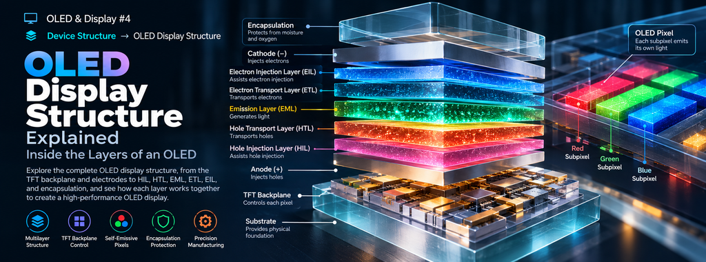
- An OLED display is built from a stack of electrodes, organic functional layers, a TFT backplane, substrate, and encapsulation structure.
- The anode and cathode supply electrical charge to the OLED device.
- HIL, HTL, EML, ETL, and EIL manage charge injection, transport, and light generation.
- The Emission Layer (EML) is the central region where excited states are formed and light is generated.
- The TFT backplane controls the electrical current delivered to individual OLED subpixels.
- Encapsulation protects the OLED stack from moisture and oxygen.
- Commercial OLED structures are more complex than simplified diagrams and may contain additional transport, blocking, or charge-generation layers.
Introduction
An OLED display may look like a single thin panel from the outside, but inside it is built from a carefully engineered stack of extremely thin layers.
Each layer performs a specific function.
Some layers inject electrical charge. Others transport electrons or holes. One region generates light, while additional structures control each pixel and protect the sensitive OLED materials from the surrounding environment.
A simplified OLED display can be understood as:
Substrate → TFT Backplane → Electrode → Organic Layers → Electrode → Encapsulation
But each of these components contains important technology of its own.
Understanding the OLED stack is essential because display performance — including brightness, efficiency, color, lifetime, and power consumption — depends on how effectively these layers work together.
The Basic Structure of an OLED Display
A simplified conventional OLED structure can be represented as:
Encapsulation
      ↓
Cathode
      ↓
Electron Injection Layer (EIL)
      ↓
Electron Transport Layer (ETL)
      ↓
Emission Layer (EML)
      ↓
Hole Transport Layer (HTL)
      ↓
Hole Injection Layer (HIL)
      ↓
Anode
      ↓
TFT Backplane
      ↓
Substrate
This is a useful learning model, but real commercial OLED structures can be significantly more complex.
Additional layers may be introduced to improve:
- Charge injection
- Charge balance
- Exciton confinement
- Efficiency
- Color performance
- Lifetime
- Optical characteristics
OLED device design is therefore best understood as a functional stack, not simply a fixed number of layers.

The Substrate: The Foundation of the Display
The OLED structure begins with the substrate.
The substrate provides the physical foundation on which the display is built.
Depending on the application, OLED displays may use different substrate materials.
Glass Substrate
Rigid OLED displays can use glass substrates.
Glass provides:
- Dimensional stability
- Smooth surfaces
- Good process compatibility
- High-temperature process tolerance
It is well suited to displays that do not need to bend.
Flexible Substrate
Flexible OLED displays commonly use thin flexible substrate structures, such as polymer-based materials.
These allow the panel to bend or curve.
Flexible substrates help enable:
- Curved displays
- Foldable smartphones
- Flexible displays
- Rollable concepts
However, replacing rigid glass with a flexible material introduces new manufacturing challenges involving dimensional stability, thermal behavior, handling, and barrier performance.
The TFT Backplane: Controlling Every Pixel
Above the substrate is the TFT backplane.
TFT stands for:
Thin-Film Transistor
The OLED material produces light, but it does not decide by itself when a pixel should turn on or how bright it should be.
That control is provided by the TFT circuitry.
A simplified relationship is:
Image Signal
     ↓
TFT Circuit
     ↓
Current Control
     ↓
OLED Subpixel
     ↓
Light
Each subpixel is connected to a pixel circuit that controls the electrical conditions applied to the OLED device.
This allows millions of subpixels across a display to be controlled independently.
Why Does the TFT Backplane Matter?
The quality of the TFT backplane directly influences display performance.
It affects:
- Pixel switching
- Current stability
- Refresh rate
- Power consumption
- Brightness uniformity
- Display resolution
Different TFT technologies are used depending on the display application.
Examples include:
LTPS
Low-Temperature Polycrystalline Silicon
Known for relatively high carrier mobility and widely used in high-resolution mobile displays.
Oxide TFT
Uses oxide semiconductor materials and can offer advantages in leakage current and large-area processing.
LTPO
Low-Temperature Polycrystalline Oxide
Combines different transistor technologies to support efficient variable refresh-rate operation.
These technologies will be explored separately later in the series.
The Anode: Injecting Holes
The first major electrode in a conventional OLED structure is the anode.
Its role is closely connected to hole injection.
When voltage is applied, holes are introduced from the anode side into the organic layers.
The anode must therefore work effectively with the neighboring organic materials.
In many OLED structures, the electrode also needs appropriate optical properties depending on whether light exits through that side of the device.
Electrode design therefore involves both:
- Electrical performance
- Optical performance
The Hole Injection Layer — HIL
Above the anode is commonly the:
Hole Injection Layer
or HIL.
Its main role is to help holes enter the organic semiconductor system efficiently.
Without effective charge injection, additional voltage may be required to operate the OLED.
The HIL helps reduce the difficulty of transferring charge from the electrode into the organic stack.
In simplified form:
Anode
  ↓
HIL
  ↓
HTL
The HIL therefore acts as an interface between the electrode and the hole-transport system.
The Hole Transport Layer — HTL
After entering the organic stack, holes move through the:
Hole Transport Layer
or HTL.
The HTL is designed to transport holes efficiently toward the emission region.
Its functions can include:
- Hole transport
- Charge balance
- Interface control
- Supporting exciton confinement
The ultimate goal is not simply to move holes quickly.
The device must deliver the right number of holes to the right region at the right time.
This makes charge balance a central part of OLED device design.
The Emission Layer — EML
At the heart of the OLED structure is the:
Emission Layer
or EML.
This is the region where light generation primarily occurs.
Electrons approach the EML from one side.
Holes approach from the other.
When they interact, excited states can form.
These excited states can release energy as photons.
In simplified form:
Electron
    ↓

   EML

    ↑
Hole

Electron + Hole
       ↓
    Exciton
       ↓
     Photon
       ↓
      Light
Because of this role, the EML is one of the most technologically important parts of an OLED device.
Host and Dopant Materials Inside the EML
The emission layer is not necessarily made from only one material.
Many OLED architectures use a host–dopant system.
Host Material
The host provides the molecular environment in which excitation energy and charge can be managed.
Dopant Material
The dopant is introduced in relatively small concentrations and can play an important role in light emission.
A simplified concept is:
Host Material
     +
Emitter / Dopant
     ↓
Controlled Light Emission
Host and dopant selection can influence:
- Efficiency
- Color
- Lifetime
- Energy transfer
- Charge balance
This is why OLED emission materials form an important specialist segment of the OLED supply chain.
The Electron Transport Layer — ETL
On the opposite side of the EML is the:
Electron Transport Layer
or ETL.
The ETL transports electrons toward the emission region.
Its role is conceptually similar to the HTL, but for electrons rather than holes.
Cathode
   ↓
EIL
   ↓
ETL
   ↓
EML
The ETL must cooperate with the rest of the OLED stack to maintain appropriate electron transport and charge balance.
Too many electrons or too few holes — or the reverse — can reduce device efficiency.
The Electron Injection Layer — EIL
Between the cathode and the ETL is commonly an:
Electron Injection Layer
or EIL.
The EIL helps electrons enter the organic semiconductor stack from the cathode.
Like the HIL on the hole side, the EIL is important because the interface between a metal electrode and an organic semiconductor can strongly affect device operation.
Efficient electron injection can help improve:
- Operating voltage
- Charge balance
- Device efficiency
The Cathode: Injecting Electrons
The cathode is the electrode associated with electron injection.
When the OLED is driven electrically, electrons enter from the cathode side and move through the electron-related organic layers toward the EML.
The simplified charge paths can now be shown together:
Cathode
   ↓
Electron Injection
   ↓
EIL
   ↓
ETL
   ↓
      EML
   ↑
HTL
   ↑
HIL
   ↑
Hole Injection
   ↑
Anode
The OLED stack therefore works by bringing two types of charge carriers toward the same emission region.
Why Are So Many Layers Necessary?
It may seem inefficient to use multiple layers when the goal is simply to generate light.
But each layer allows engineers to optimize a particular function.
A simplified division of roles is:
| Layer | Primary Function |
|---|---|
| Anode | Hole-side electrode |
| HIL | Hole injection |
| HTL | Hole transport |
| EML | Light generation |
| ETL | Electron transport |
| EIL | Electron injection |
| Cathode | Electron-side electrode |
Separating these functions allows OLED developers to tune the device more precisely.
This can improve:
- Efficiency
- Operating voltage
- Charge balance
- Brightness
- Lifetime
Real OLED Stacks Are More Complex
The simplified five-organic-layer model is useful for learning, but commercial OLED devices often contain additional functional layers.
These may include:
- Electron Blocking Layer
- Hole Blocking Layer
- Exciton Blocking Layer
- Additional transport layers
- Interface layers
- Multiple emission layers
- Charge Generation Layers
These layers can help control where charges and excitons are located inside the device.
The objective is to keep light-generating processes concentrated in the desired region while minimizing energy loss and material degradation.
Blocking Layers and Exciton Control
OLED efficiency depends not only on moving electrons and holes toward the EML, but also on preventing them from moving too far.
For example, specialized blocking layers can help limit unwanted charge or exciton movement.
Conceptually:
Electron
   ↓
[Controlled Region]

     EML

[Controlled Region]
   ↑
Hole
This helps keep the recombination zone in the desired location.
Precise control of this region can influence:
- Efficiency
- Color stability
- Lifetime
- Device reliability
Single-Stack OLED vs Tandem OLED
Not all OLED devices use only one emission unit.
Some advanced OLED structures use multiple light-emitting units stacked vertically.
This is known as a:
Tandem OLED
A simplified concept is:
Emission Unit
     ↓
Charge Generation Layer
     ↓
Emission Unit
Tandem architectures can improve certain combinations of brightness, efficiency, and lifetime.
However, they also increase:
- Stack complexity
- Material requirements
- Deposition steps
- Process control requirements
Tandem OLED will be covered in detail later in the Technologies series.
Where Does the Light Exit?
OLED architecture can also be classified by the direction in which light leaves the device.
Two important structures are:
Bottom-Emission OLED
Light exits toward the substrate side.
OLED Stack
    ↓
TFT / Substrate
    ↓
   Light
Top-Emission OLED
Light exits away from the substrate and TFT backplane.
   Light
     ↑
OLED Stack
     ↑
TFT / Substrate
Top-emission structures can offer advantages where maximizing usable emitting area is important.
However, electrode transparency, optical interference, cavity design, and material selection become important considerations.
Why Is Top Emission Important for High-Resolution Displays?
The TFT circuitry occupies physical area within a pixel.
If light must pass through the TFT side, that circuitry can constrain the available optical area.
A top-emission architecture allows light to exit from the opposite side.
This can help support a higher effective emitting area within the pixel.
That becomes especially valuable in applications requiring:
- High pixel density
- High brightness
- Compact pixel structures
Encapsulation: Protecting the OLED Stack
OLED materials cannot simply be left exposed after deposition.
The device must be protected from the environment.
This is the role of:
Encapsulation
OLED materials and electrodes can be damaged by:
- Moisture
- Oxygen
- Environmental contamination
A simplified structure is:
Environment
     ↓
Encapsulation
     ↓
OLED Device
The encapsulation system therefore creates a protective barrier around the OLED stack.
Glass Encapsulation and Thin Film Encapsulation
Different OLED designs can use different approaches to encapsulation.
Rigid Encapsulation
Rigid OLED structures can use glass-based protective approaches.
Thin Film Encapsulation — TFE
Flexible OLEDs require a barrier that can protect the device without eliminating flexibility.
TFE commonly relies on carefully engineered thin-film barrier structures.
These may combine different types of layers to achieve both:
- Barrier performance
- Mechanical flexibility
This makes TFE one of the enabling technologies behind flexible and foldable OLEDs.
How the Entire OLED Stack Works Together
The full structure can now be understood as a coordinated system.
Encapsulation
      ↓
Protect Device

Cathode
      ↓
Inject Electrons

EIL
      ↓
Assist Electron Injection

ETL
      ↓
Transport Electrons

EML
      ↓
Generate Light

HTL
      ↑
Transport Holes

HIL
      ↑
Assist Hole Injection

Anode
      ↑
Inject Holes

TFT Backplane
      ↓
Control Pixel Current

Substrate
      ↓
Provide Physical Foundation
No single layer determines OLED performance on its own.
The display works because all these structures operate together.
Structure Determines Performance
Changes in OLED layer design can affect multiple performance characteristics.
Efficiency
Better charge injection and balance can reduce energy loss.
Brightness
Material and device architecture influence how much useful light is generated and extracted.
Color
Emission-layer materials and optical structure influence emitted wavelength and color characteristics.
Lifetime
Material stability, exciton distribution, charge balance, and operating conditions affect degradation.
Power Consumption
Higher electrical and optical efficiency can reduce the energy required to produce a given level of brightness.
This is why OLED layer engineering remains a major area of research and development.
OLED Structure and Manufacturing
The OLED stack is created through multiple precision manufacturing processes.
A simplified flow includes:
TFT Backplane
      ↓
Electrode Formation
      ↓
Organic Layer Deposition
      ↓
Cathode Formation
      ↓
Encapsulation
      ↓
Inspection
The organic layers can be extremely thin.
Manufacturers therefore require precise control over:
- Film thickness
- Uniformity
- Material purity
- Deposition rate
- Pattern accuracy
- Particle contamination
- Interface quality
Small deviations can influence OLED performance.
Why Vacuum Processing Matters
Many OLED manufacturing processes are performed under vacuum.
Vacuum conditions can help:
- Control material deposition
- Reduce unwanted contamination
- Enable precise thin-film formation
- Support thermal evaporation processes
OLED device structure is therefore closely connected to vacuum equipment and thin-film deposition technology.
The stack visible in a device diagram is ultimately the result of a highly controlled manufacturing sequence.
From Device Structure to the Display Industry
Understanding the OLED stack also helps explain the industry’s supply chain.
Different parts of the structure create demand for different technologies and suppliers.
TFT Backplane
Semiconductor processing and backplane technology
Electrodes
Conductive materials and thin-film processing
HIL / HTL / ETL / EIL
Specialized organic electronic materials
Emission Layer
Host and emitter materials
Deposition
Vacuum and evaporation equipment
Encapsulation
Barrier materials and deposition equipment
Inspection
Metrology and defect-detection systems
The OLED display is therefore the result of a highly interconnected advanced-manufacturing ecosystem.
iAtlas Insight
The most important lesson from the OLED stack is that OLED competition is fundamentally a system-engineering competition.
A new emitter material can improve performance, but that material must work effectively with:
- Neighboring transport materials
- Electrodes
- Charge balance
- TFT driving conditions
- Optical architecture
- Manufacturing processes
This makes OLED development highly interdependent.
More Layers Can Create Better Performance — but More Complexity
Adding specialized functional layers can improve charge management or exciton confinement.
However, each additional layer also introduces another manufacturing variable.
That means manufacturers must balance:
Device Optimization ↔ Manufacturing Complexity
A theoretically better OLED stack is only commercially valuable if it can be produced repeatedly at acceptable yield and cost.
OLED Materials Cannot Be Evaluated in Isolation
A material that performs extremely well in one laboratory device may behave differently when integrated into another OLED architecture.
Its performance depends on:
- Energy-level alignment
- Adjacent materials
- Thickness
- Deposition conditions
- Electrical driving
- Device architecture
This is why OLED material development requires close interaction between chemical companies, panel manufacturers, and equipment suppliers.
Tandem OLED Raises the Value of Process Control
Tandem structures introduce multiple emission units and additional interfaces.
That can create performance benefits but also requires more precise deposition and stack control.
As tandem OLED expands into IT devices and other applications, process uniformity, deposition productivity, material utilization, and yield may become increasingly important.
Structure Explains the Supply Chain
Looking at an OLED layer diagram is also a way to understand the industry itself.
Each layer represents a technical requirement.
And many of those requirements correspond to a specialized supplier ecosystem.
In that sense:
The OLED stack is also a map of the OLED value chain.
FAQ
What are the main layers of an OLED?
A simplified OLED structure contains an anode, hole injection layer, hole transport layer, emission layer, electron transport layer, electron injection layer, and cathode.
Commercial OLEDs can contain additional functional layers.
Which OLED layer actually produces light?
The Emission Layer (EML) is the primary region where electron–hole interaction creates excited states that can generate light.
What does the TFT backplane do?
The TFT backplane controls the electrical current delivered to individual OLED subpixels.
It determines when a pixel turns on and how strongly it emits light.
Why does OLED need an HTL and an ETL?
The HTL transports holes toward the emission region, while the ETL transports electrons.
Together they help control where and how efficiently charges recombine.
What is the difference between HIL and HTL?
The HIL primarily assists hole injection from the electrode into the organic stack.
The HTL primarily transports those holes toward the emission layer.
What is Thin Film Encapsulation?
Thin Film Encapsulation is a barrier structure designed to protect OLED materials from moisture and oxygen while maintaining a thin and potentially flexible device structure.
Are all OLED displays built with exactly the same layers?
No.
OLED stacks vary depending on device architecture, materials, application, emission direction, and performance targets.
Simplified diagrams are useful for learning but do not represent every commercial OLED design.
Key Takeaways
- An OLED display is a multilayer electronic and optical device.
- The substrate provides the foundation, while the TFT backplane controls individual pixels.
- The anode and cathode inject holes and electrons.
- HIL and EIL assist charge injection.
- HTL and ETL transport charges toward the emission region.
- The EML is where light-generating excited states are primarily created.
- Commercial OLEDs can contain additional transport, blocking, and control layers.
- Top-emission and bottom-emission structures differ in the direction light exits the OLED.
- Encapsulation protects sensitive OLED materials from moisture and oxygen.
- OLED structure directly connects materials science, device physics, equipment, and manufacturing.
- A high-performance OLED depends on the entire stack working as a coordinated system.
OLED & Display Learning Path
Previous Article
OLED & Display #3 — How OLED Displays Work: From Electricity to Light
Current Article
OLED & Display #4 — OLED Display Structure Explained: Inside the Layers of an OLED
Next Article
OLED & Display #5 — OLED Pixels and Subpixels Explained: How Displays Create Color
The next article will examine how OLED pixels are divided into subpixels, how red, green, and blue light are controlled, and why different pixel layouts can affect resolution, brightness, lifetime, and image quality.
References & Further Reading
For this article, references should cover:
- Universal Display Corporation — Organic Light Emitting Diodes (OLEDs)
- Samsung Display — Organic Layers (HIL, HTL, EML, ETL, EIL)
- Samsung Display — Backplane
- Samsung Display — Host
- Samsung Display — Dopant
- Samsung Display — Bottom and Top Emission
ℹ️ About iAtlas
iAtlas is an independent publication covering batteries, semiconductors, OLED, advanced materials, AI, and global industrial trends.
We transform complex industrial developments into clear, reliable, and easy-to-understand insights.
Whether you’re following today’s industry news or building long-term expertise, iAtlas helps you understand not only what happened, but why it matters.
Technology creates change.
Insight creates opportunity.
— iAtlas