What Is Semiconductor Manufacturing?
💻 iAtlas Semiconductor #1 | 📘 Fundamentals → Manufacturing Overview
Introduction
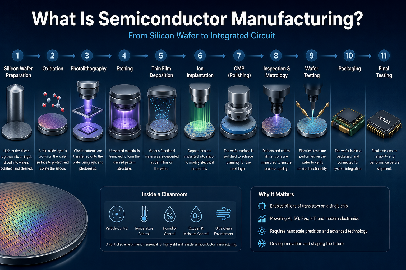
Semiconductor manufacturing is the highly advanced process of transforming a silicon wafer into thousands of integrated circuits (ICs) through hundreds of precisely controlled fabrication steps.
Every smartphone, AI server, electric vehicle, medical device, and industrial robot relies on semiconductor chips produced using this manufacturing process.
Modern semiconductor manufacturing combines nanometer-scale engineering, ultra-clean cleanrooms, advanced materials, and sophisticated automation to fabricate billions of transistors on a single silicon wafer.
Understanding semiconductor manufacturing provides the essential foundation for learning every semiconductor process covered in the iAtlas Semiconductor series.
Why It Matters
Semiconductors have become the backbone of the digital economy.
Artificial intelligence, cloud computing, autonomous driving, 5G communications, and consumer electronics all depend on increasingly advanced semiconductor manufacturing technologies.
Today’s leading-edge chips may require more than 1,000 individual process steps, each performed with nanometer-level precision.
Because every manufacturing step builds upon the previous one, understanding the complete semiconductor manufacturing process makes it much easier to learn specialized topics such as photolithography, plasma etching, atomic layer deposition (ALD), and advanced packaging.
What Is Semiconductor Manufacturing?
Semiconductor manufacturing refers to the complete fabrication process used to convert a blank silicon wafer into functional integrated circuits.
Rather than producing a single chip at a time, manufacturers fabricate hundreds or even thousands of identical chips simultaneously on one wafer before separating them into individual devices.
The overall process combines material deposition, pattern transfer, selective etching, electrical modification, polishing, inspection, and packaging to create modern semiconductor devices.
The Semiconductor Manufacturing Process
A simplified semiconductor manufacturing process typically follows these major steps:
- Silicon Wafer Preparation
- Thermal Oxidation
- Photolithography
- Etching
- Thin Film Deposition
- Ion Implantation
- Chemical Mechanical Polishing (CMP)
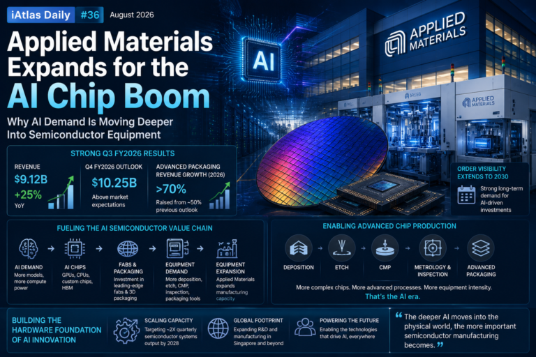
- Inspection & Metrology
- Wafer Testing
- Advanced Packaging
- Final Testing
Each manufacturing cycle adds new microscopic structures until billions of transistors are completed on a single wafer.
Step 1. Silicon Wafer Preparation
Every semiconductor begins with an ultra-pure silicon wafer.
Single-crystal silicon is grown using the Czochralski (CZ) process, sliced into thin wafers, polished to atomic-level flatness, and carefully cleaned before entering the fabrication line.
➡️ Continue reading: What Is a Silicon Wafer?
Step 2. Photolithography
Photolithography transfers microscopic circuit patterns onto the wafer using ultraviolet light and photoresist.
This process determines the dimensions and locations of transistors, making it one of the most important stages in semiconductor manufacturing.
Today’s advanced AI processors rely on Extreme Ultraviolet (EUV) lithography to produce extremely small feature sizes.
➡️ Continue reading: What Is Photolithography?
Step 3. Etching
Once the circuit pattern has been created, unwanted materials are selectively removed.
The two primary approaches are:
- Dry Etching
- Wet Etching
Modern semiconductor manufacturing primarily uses plasma-based dry etching because it provides excellent precision and anisotropic profiles.
➡️ Continue reading: Dry Etching vs. Wet Etching
Step 4. Thin Film Deposition
Multiple layers of conductive, insulating, and protective materials are deposited throughout semiconductor manufacturing.
Common deposition technologies include:
- Chemical Vapor Deposition (CVD)
- Plasma-Enhanced CVD (PECVD)
- Atomic Layer Deposition (ALD)
- Physical Vapor Deposition (PVD)
Each method is selected according to the required material properties and device structure.
Step 5. Ion Implantation
Ion implantation introduces controlled amounts of dopant atoms into silicon to modify its electrical characteristics.
This process forms the source and drain regions of transistors while enabling precise electrical control.
Step 6. Chemical Mechanical Polishing (CMP)
As additional layers accumulate, the wafer surface becomes increasingly uneven.
CMP combines chemical reactions with mechanical polishing to restore a perfectly flat surface before the next manufacturing cycle begins.
Without CMP, today’s multi-layer semiconductor devices would not be possible.
Step 7. Inspection and Metrology
Quality control takes place throughout semiconductor manufacturing.
Inspection systems detect defects, while metrology equipment measures critical parameters such as:
- Critical Dimension (CD)
- Overlay Accuracy
- Film Thickness
- Particle Contamination
Maintaining tight process control directly improves manufacturing yield.
Step 8. Advanced Packaging
After wafer fabrication is complete, chips are separated, packaged, electrically tested, and prepared for shipment.
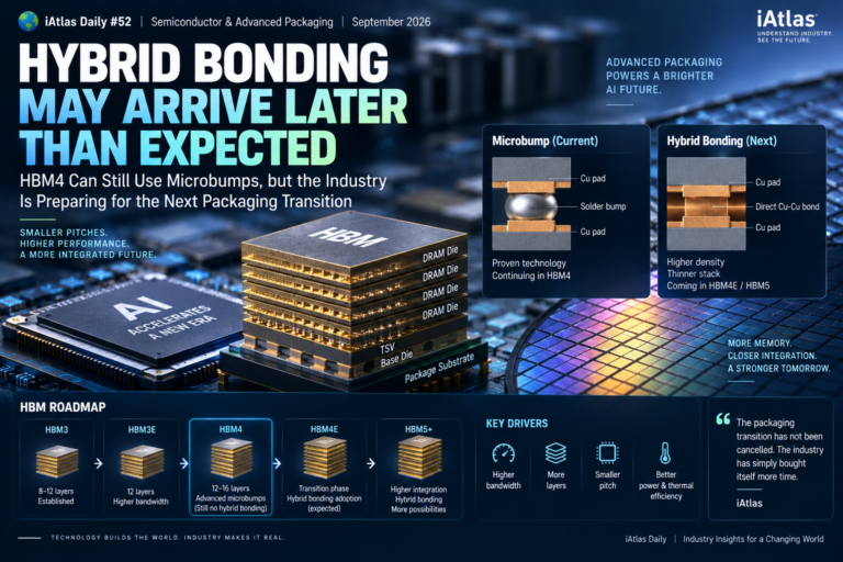
Advanced packaging technologies—including Chiplets, Through-Silicon Via (TSV), Hybrid Bonding, and High Bandwidth Memory (HBM)—have become essential for AI and high-performance computing applications.
➡️ Continue reading: Introduction to Advanced Packaging
Why Cleanrooms Matter
Semiconductor manufacturing takes place inside highly controlled cleanrooms where airborne particles, temperature, humidity, oxygen, and moisture are carefully regulated.
Even microscopic contamination can reduce manufacturing yield or damage integrated circuits.
For advanced research and specialized processes, inert environments and moisture-free handling systems are also required to protect highly sensitive materials.
Looking Ahead
The future of semiconductor manufacturing will be shaped by:
- High-NA EUV Lithography
- 3D Integration
- Chiplet Architectures
- AI-driven Manufacturing
- Advanced Packaging
- Smart Factories
These technologies will continue driving improvements in computing performance, power efficiency, and manufacturing productivity.
Key Takeaways
- Semiconductor manufacturing transforms silicon wafers into integrated circuits through hundreds of precision fabrication steps.
- Photolithography, etching, deposition, ion implantation, and CMP form the foundation of modern chip manufacturing.
- Cleanroom environments are essential for maintaining manufacturing yield and product reliability.
- Advanced packaging technologies have become as important as wafer fabrication for AI computing.
📖 Semiconductor Learning Path
Current: 💻 Semiconductor #1 | What Is Semiconductor Manufacturing?
Next: 💻 Semiconductor #2 | What Is a Silicon Wafer?
📚 Continue Reading
- 💻 Semiconductor #2 | What Is a Silicon Wafer?
- 💻 Semiconductor #3 | How the Czochralski (CZ) Process Works
- 💻 Semiconductor #4 | What Is Photolithography?
- 💻 Semiconductor #5 | Dry Etching vs. Wet Etching
- 💻 Semiconductor #6 | Introduction to Advanced Packaging
References
🔷 About iAtlas
iAtlas is an independent publication covering batteries, semiconductors, OLED, advanced materials, AI, and global industrial trends.
We transform complex industrial developments into clear, reliable, and easy-to-understand insights.
Whether you’re following today’s industry news or building long-term expertise, iAtlas helps you understand not only what happened, but why it matters.
Technology creates change.
Insight creates opportunity.
— iAtlas