Applied Materials and Intel Are Rethinking Next-Generation Chipmaking
Inside the $5 Billion EPIC Center and the New Collaboration Model for Transistors, Interconnects, and Advanced Packaging
iAtlas Daily #78 | Semiconductor & Manufacturing Technology | October 15, 2026
The Big Story
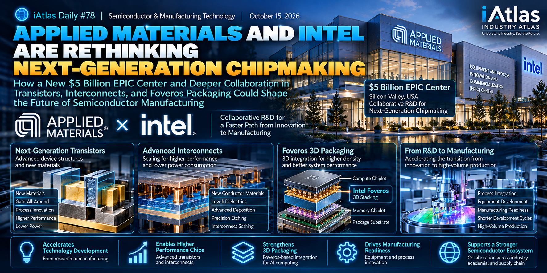
The Applied Materials Intel partnership is bringing semiconductor equipment development and chip manufacturing research closer together, as the industry searches for faster ways to develop next-generation technologies for AI computing.
On October 6, 2026, Applied Materials announced an expanded collaboration with Intel focused on advanced transistors, interconnects, and semiconductor packaging.
The companies will combine research capabilities at Applied Materials’ Equipment and Process Innovation and Commercialization (EPIC) Center in Silicon Valley and Intel’s research campus in Hillsboro, Oregon.
Just days later, on October 12, Applied Materials unveiled its $5 billion EPIC Center, positioning the facility as a major investment in collaborative semiconductor process technology and equipment research.
Together, these announcements point to a change in how semiconductor innovation is organized.
Instead of developing equipment, materials, and chip architectures through largely separate processes, manufacturers and technology suppliers are increasingly seeking to work together earlier.
The objective is not simply to invent better semiconductor technologies. It is to reduce the time required to turn those inventions into reliable manufacturing processes.
1. What Applied Materials and Intel Announced
The collaboration spans several areas of advanced semiconductor manufacturing.
| Area | Research Focus |
|---|---|
| Transistors | Next-generation materials, device structures, and processes |
| Interconnects | Advanced wiring and interconnect scaling |
| Front-end manufacturing | Logic-device fabrication technologies |
| Back-end-of-line | Metal interconnects and associated processes |
| Advanced packaging | Foveros-based 3D stacking |
| Power delivery | Improved electrical performance |
| Thermal management | Managing heat in high-performance systems |
| Manufacturing transition | Shortening development and qualification cycles |
Intel is participating as a founding partner of the EPIC Center.
The collaboration builds on the companies’ existing relationship in semiconductor process technology development.
However, the announcements do not establish a specific new commercial chip, production-node launch date, or guaranteed performance improvement.
The immediate focus is research and development.
That distinction matters because successful semiconductor manufacturing requires years of process development, integration, testing, and qualification.
2. Why the $5 Billion EPIC Center Matters
The EPIC Center represents a significant investment in the semiconductor innovation process itself.
Applied Materials describes the facility as a collaborative research environment where semiconductor manufacturers, equipment companies, systems developers, and academic researchers can work together.
Its purpose is to accelerate the transition from early-stage technology development to high-volume manufacturing.
Traditionally, semiconductor process innovation can involve multiple development stages.
Research Concept → Materials Development → Equipment Development → Process Integration → Qualification → High-Volume Manufacturing
Each transition introduces technical challenges.
A promising material may not perform consistently in a manufacturing environment.
A new device architecture may require additional deposition, etching, or inspection capabilities.
An equipment process may work independently but create unexpected problems when integrated with other manufacturing steps.
The EPIC Center is designed to bring more of these activities into a shared development environment.
This could help engineers identify integration problems earlier and reduce repeated development cycles.
The potential advantage is particularly important as advanced semiconductor manufacturing becomes more expensive and complex.
3. Transistor Innovation Is Becoming a Materials Challenge
For decades, semiconductor progress has been associated with smaller transistor dimensions.
But reducing feature sizes is no longer sufficient by itself to deliver the performance and power-efficiency improvements demanded by AI computing.
Modern transistor development increasingly depends on new device architectures and advanced materials engineering.
Intel and Applied Materials are collaborating on next-generation device structures and manufacturing processes.
These efforts are relevant to the broader industry’s transition toward increasingly complex transistor architectures.
For example, gate-all-around transistor designs use a gate structure surrounding the channel to improve electrostatic control.
Further improvements may require new channel materials, contact technologies, dielectric layers, and integration methods.
Each change can create additional manufacturing challenges.
A new material must be deposited or formed precisely.
Interfaces must remain stable.
Defects must be controlled.
And the resulting devices must meet electrical and reliability requirements.
This makes equipment suppliers increasingly important participants in transistor innovation.
Future transistor performance will depend not only on device design, but also on the ability to manufacture advanced materials with extremely high precision.
4. Interconnects Are Becoming a Critical Performance Constraint
Transistors perform computation, but interconnects allow signals and power to move through a semiconductor device.
As transistor density increases, the complexity of the wiring network also grows.
Interconnect scaling presents several challenges.
These include electrical resistance, capacitance, signal delay, power consumption, and manufacturing complexity.
Even when transistors become faster, interconnect limitations can reduce the performance benefits of scaling.
The Applied Materials Intel collaboration specifically includes front-end and back-end-of-line technologies, including interconnect scaling.
This is important because advanced interconnect development involves multiple manufacturing disciplines.
Potential areas of innovation include conductor materials, dielectric materials, deposition, etching, planarization, and process integration.
The exact technologies selected under the collaboration have not been fully disclosed.
Nevertheless, the strategic direction is clear.
Semiconductor performance increasingly depends on optimizing the complete device structure rather than improving transistors in isolation.
5. Foveros and the Future of 3D Packaging
Another important part of the collaboration involves Intel’s Foveros-based advanced packaging technologies.
Foveros enables the integration of multiple semiconductor components through three-dimensional stacking architectures.
This approach can help manufacturers combine different functions and process technologies within a single package.
The collaboration aims to advance packaging capabilities involving higher interconnect density, improved power delivery, and better thermal performance.
These requirements are particularly relevant to high-performance AI computing.
As more computing functions are integrated into advanced packages, manufacturers must manage increasingly complex electrical and thermal interactions.
3D stacking can provide significant integration advantages, but it also introduces manufacturing challenges.
These include bonding accuracy, interconnect reliability, heat dissipation, wafer handling, and defect control.
The ability to address these challenges at scale will influence the commercial success of future packaging architectures.
Advanced packaging is therefore becoming a central part of semiconductor technology development, rather than a separate downstream activity.
6. Why AI Is Changing the Semiconductor R&D Model
AI infrastructure is increasing demand for computing performance, memory bandwidth, and energy efficiency.
Meeting these requirements involves more than producing additional semiconductor wafers.
It requires progress across multiple technologies.
Transistors determine the performance and efficiency of individual devices.
Interconnects influence communication and power delivery within chips.
Advanced packaging enables integration across multiple semiconductor components.
Thermal management helps maintain performance as power density increases.
These technologies interact.
A change in packaging architecture may affect power delivery requirements.
A new transistor design may require different materials and process equipment.
Higher interconnect density may introduce additional thermal or reliability challenges.
Developing these technologies independently can increase the risk of integration problems.
Collaborative R&D provides an opportunity to evaluate those interactions earlier.
The EPIC Center reflects this approach by bringing different participants in the semiconductor ecosystem into a shared innovation environment.
7. What This Means for Semiconductor Equipment Suppliers
The Applied Materials Intel collaboration highlights the changing role of semiconductor equipment manufacturers.
Equipment suppliers have traditionally been evaluated through factors such as process performance, productivity, cost of ownership, and reliability.
Those factors remain essential.
But equipment companies are also becoming increasingly involved in early-stage device and process development.
| Equipment Technology | Potential Development Role |
|---|---|
| Deposition | Creating advanced materials and thin films |
| Etching | Forming increasingly complex device structures |
| Materials modification | Controlling material properties and interfaces |
| Planarization | Supporting multilayer integration |
| Metrology | Measuring critical dimensions and material properties |
| Inspection | Identifying defects during process development |
| Packaging equipment | Enabling advanced bonding and 3D integration |
These are relevant manufacturing technology categories, not confirmed equipment orders associated with the partnership.
For suppliers, earlier involvement in customer R&D may provide a better understanding of future manufacturing requirements.
For chipmakers, closer collaboration may improve process integration and reduce development risks.
The commercial value of this model will depend on whether it produces measurable improvements in development speed, manufacturing yield, and technology readiness.
8. The Broader Shift Toward Collaborative Semiconductor Innovation
The Intel partnership is part of a wider industry movement.
Applied Materials has also announced collaborations involving advanced packaging, memory, and other semiconductor technologies.
This reflects the increasing complexity of the semiconductor manufacturing roadmap.
No single company controls every technology required to manufacture a leading-edge computing system.
Chip designers, foundries, memory manufacturers, equipment suppliers, materials companies, and packaging specialists must coordinate across increasingly complex technical interfaces.
The EPIC Center provides one model for organizing that cooperation.
However, collaborative research does not eliminate competition.
Companies still need to protect intellectual property, differentiate their manufacturing technologies, and qualify processes for their own production requirements.
The challenge is to accelerate shared technology development while maintaining the commercial and technical boundaries required by each participant.
Industry Impact
Semiconductor manufacturers: Earlier collaboration with equipment suppliers could reduce development risks and accelerate process qualification.
Equipment suppliers: Participation in device and architecture development may increase their strategic importance in the semiconductor value chain.
Materials companies: New transistor and interconnect architectures could create demand for advanced materials and tighter process control.
Advanced packaging companies: Continued development of 3D integration may expand opportunities in bonding, inspection, and thermal-management technologies.
AI chip developers: Improvements in transistor performance, interconnect efficiency, and packaging integration could support future computing systems.
U.S. semiconductor ecosystem: Collaborative research infrastructure may strengthen domestic capabilities in advanced process development and manufacturing technology.
What to Watch
EPIC Center research milestones
Watch for announcements identifying specific technologies developed through the new collaboration.
Intel’s manufacturing roadmap
Progress in advanced logic and packaging technologies will help demonstrate whether research outcomes are moving toward production.
Foveros development
Higher interconnect density, power delivery, and thermal performance will remain important areas to monitor.
New materials and equipment platforms
Future product announcements may reveal how collaborative research translates into manufacturing capabilities.
Commercial qualification
The most meaningful evidence of success will be technologies qualified for high-volume manufacturing.
Additional research partnerships
New collaborations could indicate whether the EPIC Center model is expanding across the semiconductor industry.
iAtlas Insight
The Applied Materials Intel partnership represents more than another semiconductor research agreement.
It reflects a structural change in how the industry approaches technological progress.
As semiconductor architectures become more complex, innovation can no longer be measured only by the performance of individual devices.
Transistors, interconnects, packaging, power delivery, and thermal management must work together.
That increases the importance of process integration.
It also changes the role of equipment manufacturers.
Instead of supplying tools after a manufacturing process has been defined, equipment companies are becoming more deeply involved in shaping the technologies that future processes will require.
The $5 billion EPIC Center is an investment in this collaborative development model.
Its success will ultimately depend on whether it helps transform promising technologies into commercially viable manufacturing processes.
The next semiconductor advantage may come not only from developing better chips, but from developing a faster and more effective system for manufacturing them.
That could become one of the defining competitive factors in the AI semiconductor era.
Related Articles
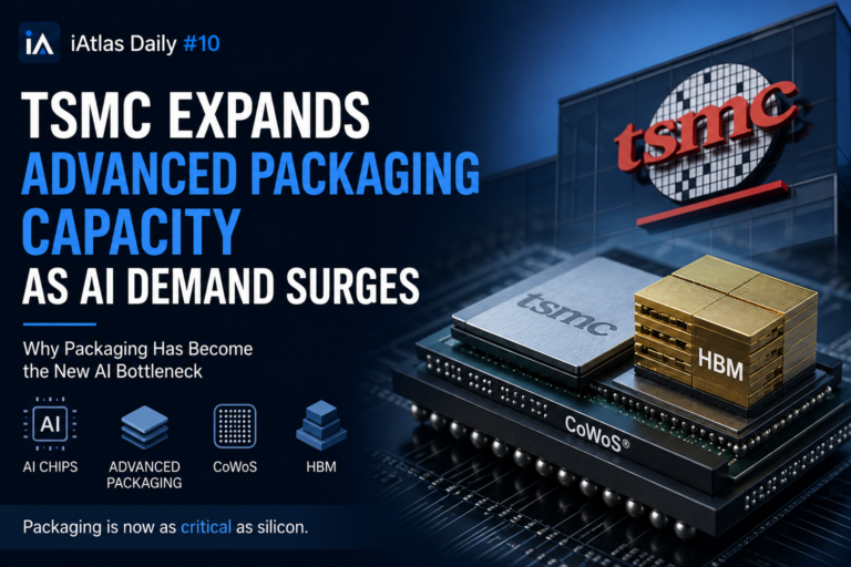
TSMC Expands Advanced Packaging Capacity as AI Demand Grows
Explore why growing AI demand is driving investment in advanced semiconductor packaging capacity.
AI Data Center Infrastructure: The Next Industrial Investment Cycle
Understand how AI infrastructure growth is creating demand across semiconductors, electricity, and industrial equipment.
References
1. Applied Materials — Official Announcement (October 6, 2026)
Applied Materials and Intel Collaborate to Accelerate Chipmaking Innovations for AI-Driven Computing.
2. Applied Materials — Official Announcement (October 12, 2026)
Applied Materials Unveils $5 Billion EPIC Center in Silicon Valley to Accelerate Semiconductor Innovation for the AI Era.
3. Applied Materials — Investor Relations (October 6, 2026)
Applied Materials and Intel Collaborate to Accelerate Chipmaking Innovations.
4. Applied Materials Korea — Official Announcement (October 7, 2026)
Applied Materials and Intel Collaborate to Accelerate Chipmaking Innovations for AI Computing.
ℹ️ About iAtlas
iAtlas is an independent publication covering batteries, semiconductors, OLED, advanced materials, AI, and global industrial trends.
We transform complex industrial developments into clear, reliable, and easy-to-understand insights.
Whether you’re following today’s industry news or building long-term expertise, iAtlas helps you understand not only what happened, but why it matters.
Technology creates change.
Insight creates opportunity.
— iAtlas