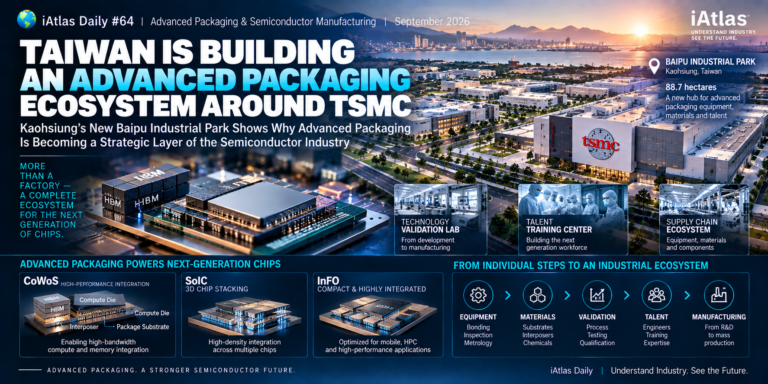
Taiwan Is Building an Advanced Packaging Ecosystem Around TSMC
Kaohsiung’s New Baipu Industrial Park Shows Why Advanced Packaging Is Becoming a Strategic Layer of the Semiconductor Industry 🔲 iAtlas Daily #64 | Advanced Packaging & Semiconductor Manufacturing | September 2026 For decades, semiconductor manufacturing was dominated by one fundamental race: Make Transistors Smaller Smaller transistors enabled: More Computing Power Higher Density Better Energy Efficiency…