
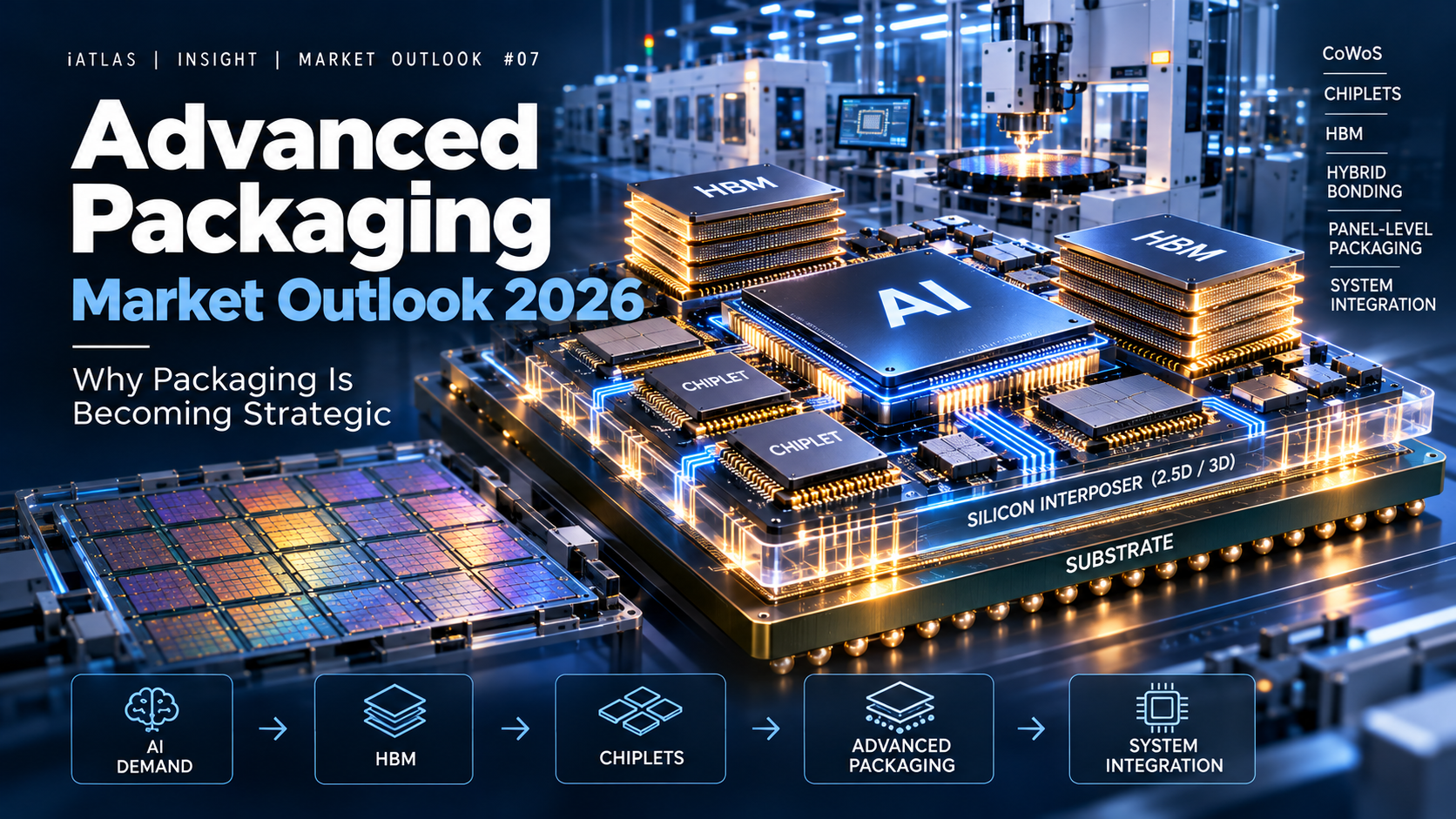
Advanced Packaging Market Outlook 2026
Why Packaging Is Becoming Strategic
iAtlas | Insight | Market Outlook #07
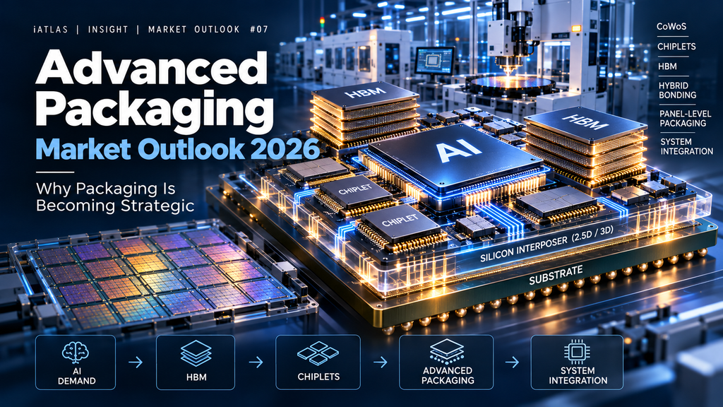
The advanced packaging market outlook for 2026 points to a fundamental change in how semiconductor performance is created.
For decades, the industry’s most important performance improvements came primarily from making transistors smaller.
That strategy remains critical.
But AI accelerators are becoming so large, memory-intensive and power-hungry that transistor scaling alone is no longer enough.
Modern AI processors increasingly combine:
Leading-Edge Logic
HBM
Chiplets
High-Speed Interconnects
Advanced Substrates
inside a single package.
That makes packaging part of the semiconductor architecture itself.
SEMI expects semiconductor assembly and packaging equipment sales to rise to approximately $6.7 billion in 2026, supported by increasingly complex AI and HBM devices.
Meanwhile, TSMC, Intel, ASE and Amkor are expanding technologies and manufacturing capacity designed specifically for increasingly large, complex AI packages.
The result is a structural shift:
Packaging is no longer simply the final step after chip manufacturing.
It is becoming one of the technologies that determines how powerful the chip system can become.
Key Takeaways
- AI and HBM are making advanced packaging a strategic semiconductor bottleneck.
- SEMI forecasts assembly and packaging equipment sales of approximately $6.7 billion in 2026, up about 9.6% year over year.
- TSMC is already producing approximately 5× reticle-size CoWoS packages and is developing 9× and 14× reticle-size solutions for larger AI systems.
- Chiplets and heterogeneous integration allow manufacturers to combine different technologies rather than build one enormous monolithic die.
- HBM makes packaging particularly important because memory must sit extremely close to AI processors.
- Technologies including CoWoS, Foveros, EMIB, hybrid bonding and panel-level packaging are becoming more strategically important.
- ASE plans to bring its automated 310 mm × 310 mm panel-level packaging line into production in the first half of 2027.
- Amkor has expanded its planned Arizona advanced-packaging investment to approximately $12 billion, reflecting strong demand for U.S.-based capacity.
- The next packaging challenges extend beyond interconnect density to power delivery, thermal management, test and yield.
- Advanced packaging is increasingly blurring the boundary between front-end semiconductor manufacturing and traditional back-end assembly.
1. Why Traditional Scaling Is No Longer Enough
For decades, semiconductor progress followed a relatively straightforward model.
Make transistors smaller.
Put more of them onto a chip.
Increase performance.
Reduce power per transistor.
This remains the foundation of advanced semiconductor manufacturing.
But AI is pushing chip design toward physical and economic limits.
An advanced AI accelerator can require enormous amounts of:
- Compute
- Memory bandwidth
- I/O
- Power
- Die area
Building all of those functions onto one gigantic piece of silicon becomes increasingly difficult.
Large dies are expensive.
They are harder to manufacture at high yield.
And individual lithography exposures have physical size limits.
This creates a new problem:
How can semiconductor companies continue scaling computing systems when one chip is no longer enough?
The answer increasingly lies in advanced packaging.
2. From One Big Chip to a System of Chips
The industry is gradually moving away from relying exclusively on one monolithic processor.
Instead, different functions can be separated into smaller dies or chiplets.
For example:
Compute Chiplet
I/O Chiplet
Cache
HBM
Specialized Accelerator
can be integrated into one semiconductor package.
Each component can potentially use the process technology best suited to its function.
Advanced logic might use a leading-edge node.
I/O may use a more mature node.
HBM is manufactured using advanced DRAM technology.
Other specialized components can use different processes entirely.
Packaging then connects them together.
Intel describes this approach as moving from one large chip toward a system of interconnected silicon tiles, using technologies such as Foveros and EMIB.
This changes the role of packaging.
Instead of simply protecting a finished semiconductor die, packaging increasingly determines how multiple dies communicate as one computing system.
3. AI Is Accelerating the Transition
AI is one of the strongest drivers of this shift.
An AI accelerator requires enormous computing power.
But compute alone cannot solve the problem.
AI processors also require extremely high memory bandwidth.
That is why HBM has become critical.
A simplified AI package now looks like:
AI Accelerator
↓
Multiple HBM Stacks
↓
High-Density Interconnect
↓
Interposer / Advanced Substrate
↓
Advanced Package
The processor and memory must communicate across extremely short, high-bandwidth connections.
Traditional PCB-level connections are insufficient for the highest-performance systems.
Advanced packaging brings the components much closer together.
That reduces communication distance and enables dramatically higher bandwidth.
The relationship is therefore direct:
More Powerful AI Accelerators
↓
More HBM
↓
Larger Packages
↓
More Complex Interconnects
↓
Greater Advanced Packaging Demand
This is why HBM growth and advanced packaging growth are inseparable.
4. CoWoS Has Become Critical AI Infrastructure
One of the best-known technologies in this market is TSMC’s CoWoS — Chip-on-Wafer-on-Substrate.
CoWoS is designed to integrate advanced logic and memory within a high-performance package.
TSMC offers several variants — including CoWoS-S, CoWoS-L and CoWoS-R — for different system requirements.
AI accelerators have dramatically increased demand for these technologies because GPUs and custom AI ASICs increasingly require multiple HBM stacks surrounding the compute die.
But the packages themselves are becoming larger.
TSMC said in October 2026 that it was already producing approximately 5× reticle-size advanced packages with strong yield, while working toward 9× and eventually 14× reticle-size packaging.
This is an important indicator.
The AI industry is not simply asking for faster individual chips.
It is asking semiconductor manufacturers to build increasingly large systems of chips inside one package.
5. HBM Is Making Packaging More Valuable
HBM reinforces this trend because it cannot simply be installed like conventional memory modules.
Multiple DRAM dies are stacked vertically.
Those HBM stacks must then sit close to the AI processor.
The resulting system requires:
- Very high interconnect density
- Short signal paths
- High-quality substrates
- Precise assembly
- Advanced thermal management
- Sophisticated testing
As discussed in Market Outlook #06, HBM4 is also making the relationship even more complex because the base die increasingly contains logic functionality.
The value chain begins to converge:
Advanced Logic
HBM
Foundry
Packaging
Instead of separate semiconductor industries operating independently, these technologies increasingly need to be developed together.
That is one reason advanced packaging has become strategically important.
6. Chiplets Could Change Semiconductor Economics
Chiplets offer another important advantage.
Large monolithic chips become increasingly difficult to manufacture because a defect anywhere on the die can reduce yield.
Smaller dies can potentially improve manufacturing efficiency.
Consider a simplified example.
Instead of manufacturing one massive processor:
One Large Die
companies can manufacture:
Compute Die A + Compute Die B + I/O Die + Cache Die
and combine them inside an advanced package.
This creates several potential benefits:
- Better manufacturing yield
- Greater design flexibility
- Reuse of proven chiplets
- Faster product development
- Ability to mix different process nodes
- Potential cost optimization
TSMC highlights similar benefits for chiplet-based networking products using its InFO packaging technologies, including architectural flexibility, design reuse and improved logic yield.
This suggests advanced packaging may eventually become not simply a performance technology but an important semiconductor cost-management tool.
7. Intel Is Betting on Foveros and EMIB
TSMC is not the only company developing advanced packaging aggressively.
Intel has built a portfolio around technologies including:
EMIB
for connecting dies horizontally.
and
Foveros
for vertical 3D stacking.
Intel describes EMIB as using small silicon bridges embedded within the substrate rather than relying on a large silicon interposer across the entire package.
The company’s newest EMIB-T technology also incorporates through-silicon features intended to improve power delivery and signal routing for increasingly demanding HBM-based systems.
Intel says its advanced packaging technology currently supports packages far larger than conventional reticle limits and is targeting further expansion by 2028.
The strategic significance goes beyond Intel’s own processors.
Intel Foundry is positioning packaging as a service that could attract external semiconductor customers.
In June 2026, Intel reorganized advanced packaging and system integration under dedicated Foundry leadership, explicitly describing packaging as a defining capability for next-generation computing systems.
This is another sign that packaging is becoming part of foundry competition itself.
8. Hybrid Bonding Is Moving Toward the Center
As packages become denser, traditional connection technologies face limits.
One important emerging technology is hybrid bonding.
Instead of relying only on relatively large solder bumps, hybrid bonding can create extremely fine-pitch connections between semiconductor surfaces.
That allows:
- Higher interconnect density
- Shorter communication distance
- Lower power consumption
- Greater vertical integration
Hybrid bonding can be especially important in:
3D Logic
Memory Stacking
Chiplets
Future HBM Architectures
SEMI identifies hybrid bonding as one of the central technologies advancing heterogeneous integration in the AI era.
As more semiconductor functionality moves vertically, bonding technology becomes increasingly important.
This pushes packaging closer to wafer-fabrication precision.
9. Panel-Level Packaging Could Improve Economics
Another major development is panel-level packaging.
Most semiconductor processing traditionally uses circular wafers.
But increasingly large AI packages use a growing portion of that circular area inefficiently.
A square panel can potentially improve material utilization.
ASE announced an automated 310 mm × 310 mm panel-level packaging platform in May 2026.
The system extends its FOCoS and FOCoS-Bridge technologies from wafer-level production toward larger square panels.
ASE expects the line to enter production during the first half of 2027.
The logic is relatively straightforward.
Larger AI Packages
↓
Less Efficient Wafer Utilization
↓
Larger Square Panels
↓
More Packages per Manufacturing Area
↓
Potential Cost Improvement
Panel-level packaging is therefore becoming increasingly interesting as advanced packages grow physically larger.
But manufacturing large panels also creates difficult engineering challenges around:
- Warpage
- Uniformity
- Fine-line patterning
- Alignment
- Handling
- Yield
Solving these problems could significantly change advanced-packaging economics.
10. Package Size Is Becoming a New Scaling Metric
Historically, semiconductor progress was frequently measured by transistor dimensions:
10 nm
↓
7 nm
↓
5 nm
↓
3 nm
↓
2 nm
That metric remains extremely important.
But AI introduces another scaling dimension:
package size.
TSMC’s move from roughly 5× to 9× and ultimately 14× reticle-scale package ambitions illustrates the direction.
Larger packages allow more:
- Logic dies
- HBM stacks
- Chiplets
- I/O
- Interconnect bandwidth
to operate together.
Future AI performance may therefore increasingly depend on two simultaneous scaling paths:
Transistor Scaling
System Scaling
Advanced packaging sits at the center of the second.
11. Power Delivery Is Becoming a Packaging Problem
Connecting more chips is only one challenge.
Those chips must also receive enormous amounts of power.
AI accelerators are becoming some of the most power-intensive semiconductor systems ever produced.
Traditional board-level power-delivery architectures create resistance and energy loss as current travels from voltage regulators toward the processor.
Packaging companies are therefore bringing power components closer to compute.
ASE, for example, introduced an expanded PowerSiP architecture in October 2026 using vertically integrated voltage-regulator modules.
ASE says the approach can reduce parasitic routing losses by 50% or more by shortening high-current transmission paths.
This illustrates another major change:
Packaging increasingly affects not only data communication, but also power architecture.
12. Thermal Management Is Becoming Critical
Where there is more computing power, there is more heat.
AI packages combine:
- Large processors
- Multiple HBM stacks
- Dense interconnects
- High power consumption
within a relatively small physical area.
This creates difficult thermal-management challenges.
Heat can affect:
- Performance
- Reliability
- Memory stability
- Interconnect integrity
- Component lifetime
As packages become larger and more three-dimensional, cooling becomes increasingly complex.
SEMI identifies power delivery and thermal management as core themes in the next generation of advanced packaging development.
The package can therefore no longer be designed independently of the system.
Future semiconductor development increasingly requires:
Chip Design
Packaging
Power
Cooling
to be co-designed.
13. Test and Yield Become More Difficult
Advanced packaging creates another challenge that receives less public attention:
testing.
A package can contain several expensive components.
Imagine combining:
- Advanced GPU
- Multiple HBM stacks
- I/O dies
- Chiplets
- Advanced substrate
If one component fails late in the manufacturing process, the economic loss can be substantial.
That makes known-good-die testing, inspection and process control extremely important.
SEMI forecasts continued growth in test-equipment investment alongside advanced packaging as AI and HBM devices become more complex.
Inspection and metrology also become more difficult as interconnect dimensions shrink and packages become increasingly three-dimensional.
Packaging yield may therefore become one of the most important hidden variables affecting AI semiconductor cost.
14. OSAT Companies Are Moving Up the Value Chain
The rise of advanced packaging also changes the competitive position of traditional semiconductor assembly and test companies, or OSATs.
Historically, the most valuable parts of the semiconductor supply chain were often considered:
Chip Design
and
Wafer Fabrication
while packaging was viewed as a lower-value manufacturing activity.
That hierarchy is changing.
Companies such as ASE and Amkor increasingly provide technically sophisticated integration platforms.
Amkor’s recent investments illustrate the scale of the change.
In September 2026, the company expanded its planned Arizona advanced-packaging and test campus to approximately 93,000 square meters of cleanroom space and increased total planned investment to approximately $12 billion.
In October, Amkor announced additional South Korean capacity commitments with NVIDIA, bringing the companies’ multi-year agreements across Arizona and Korea to approximately $3 billion.
These are no longer small back-end facilities.
They are becoming strategic AI infrastructure.
15. Advanced Packaging Is Also Becoming Geopolitical
The semiconductor localization trend previously focused heavily on wafer fabs.
That is no longer sufficient.
If a country manufactures advanced chips domestically but must send them abroad for critical packaging, the supply chain remains geographically dependent.
This is one reason advanced-packaging capacity is increasingly part of semiconductor industrial policy.
TSMC is investing in additional advanced-packaging facilities alongside leading-edge manufacturing, including major capacity expansion in Taiwan and planned U.S. investment.
Amkor is expanding in both the United States and Korea.
Intel is expanding advanced packaging in New Mexico.
ASE continues investing in next-generation packaging technologies in Asia.
The localization question is therefore expanding from:
Where are wafers manufactured?
to:
Where can the entire advanced semiconductor system be manufactured and integrated?
16. Packaging Is Blurring the Front-End / Back-End Boundary
Traditional semiconductor manufacturing was clearly divided.
Front End
Transistor fabrication
Wafer processing
Lithography
Etching
Deposition
Back End
Packaging
Assembly
Test
Advanced packaging makes that distinction less clear.
Processes increasingly require:
- Wafer-level fabrication
- Extremely fine interconnects
- TSV
- Hybrid bonding
- Advanced lithography
- Complex materials
- High-precision metrology
These resemble front-end semiconductor processes much more than traditional packaging.
The industry is therefore moving toward a continuum:
Wafer Fabrication
↓
Wafer-Level Integration
↓
Advanced Packaging
↓
System Integration
The physical boundary between chip manufacturing and packaging is becoming increasingly blurred.
17. The Advanced Packaging Equipment Market Is Growing
These technology changes are translating directly into equipment demand.
SEMI expects semiconductor assembly and packaging equipment sales to reach approximately $6.7 billion in 2026, representing about 9.6% year-over-year growth.
By 2028, SEMI forecasts the market could reach approximately $8.6 billion.
Growth is being supported by increasingly complex:
- AI processors
- HBM
- Chiplets
- 2.5D packages
- 3D integration
- Heterogeneous systems
But equipment demand extends far beyond traditional assembly tools.
Advanced packaging increasingly requires:
Bonding
Lithography
Metrology
Inspection
Wafer Thinning
Plating
Etching
Cleaning
Testing
This creates opportunities across a much broader semiconductor equipment ecosystem.
18. The Next Packaging Frontier Could Be Optical
Another technology is beginning to move closer to advanced packaging:
optics.
As AI clusters grow, electrical interconnects face increasing power and bandwidth constraints.
One possible solution is bringing optical communication increasingly close to — or directly into — semiconductor packages.
This concept is commonly described as co-packaged optics.
SEMI identifies co-packaged optics and photonic integration among the important areas being developed for future high-volume advanced packaging.
If optical links move closer to processors, packaging would become responsible for integrating:
Logic
Memory
Power
Optics
inside increasingly complex systems.
That would move packaging even further away from its traditional role.
iAtlas Outlook
The advanced packaging market outlook suggests the semiconductor industry is entering a new era of system-level scaling.
For decades, industry progress was dominated by transistor scaling.
Semiconductor Scaling 1.0
Smaller Transistors
↓
More Transistors
↓
Faster Chips
↓
Better Performance
That model is evolving.
Semiconductor Scaling 2.0
Advanced Logic
↓
Chiplets
↓
HBM
↓
2.5D / 3D Integration
↓
Advanced Packaging
↓
System-Level Performance
The distinction is important.
The future of semiconductor performance will not depend only on how small a transistor becomes.
It will increasingly depend on how effectively multiple semiconductor technologies can be integrated together.
That changes where value is created.
Foundries need advanced packaging.
Memory companies need packaging.
AI-chip designers need packaging.
OSAT companies are moving toward higher-value integration.
Equipment companies are developing new processes.
And governments are beginning to treat packaging capacity as part of strategic semiconductor infrastructure.
The competitive advantage of the next generation of semiconductors may therefore come from three capabilities working together:
Leading-Edge Process Technology
Advanced Memory
Advanced Packaging
AI is accelerating that convergence.
And as AI systems become larger, hotter, more memory-intensive and more heterogeneous, packaging will become even more important.
Advanced packaging is no longer simply about putting a chip inside a package.
It is becoming about building the computing system itself.
That is why packaging is becoming strategic.
Continue Reading
Previous Market Outlook
HBM Market Outlook 2026
Why AI Is Reshaping the Memory Market
Next Market Outlook
AI Semiconductor Market Outlook 2026
Beyond GPUs: How AI Is Reshaping the Chip Industry
References
SEMI — Global Semiconductor Equipment Forecast 2026–2028
Advanced packaging, test and semiconductor equipment investment outlook.
TSMC — 3DFabric / CoWoS Technology
CoWoS-S, CoWoS-L, CoWoS-R and heterogeneous integration roadmap.
Intel Foundry — Advanced Packaging for AI Semiconductors
EMIB, EMIB-T and Foveros packaging technologies.
ASE — 310 mm × 310 mm Panel-Level Packaging
Panel-level packaging roadmap for large AI and heterogeneous packages.
Amkor — Arizona Advanced Packaging and Test Campus
Expansion of U.S. advanced-packaging manufacturing capacity.
Amkor — NVIDIA Advanced Packaging Partnership
Advanced-packaging capacity expansion in the United States and South Korea.
ℹ️ About iAtlas
iAtlas is an independent publication covering batteries, semiconductors, OLED, advanced materials, AI, and global industrial trends.
We transform complex industrial developments into clear, reliable, and easy-to-understand insights.
Whether you’re following today’s industry news or building long-term expertise, iAtlas helps you understand not only what happened, but why it matters.
Technology creates change.
Insight creates opportunity.
— iAtlas

One Comment