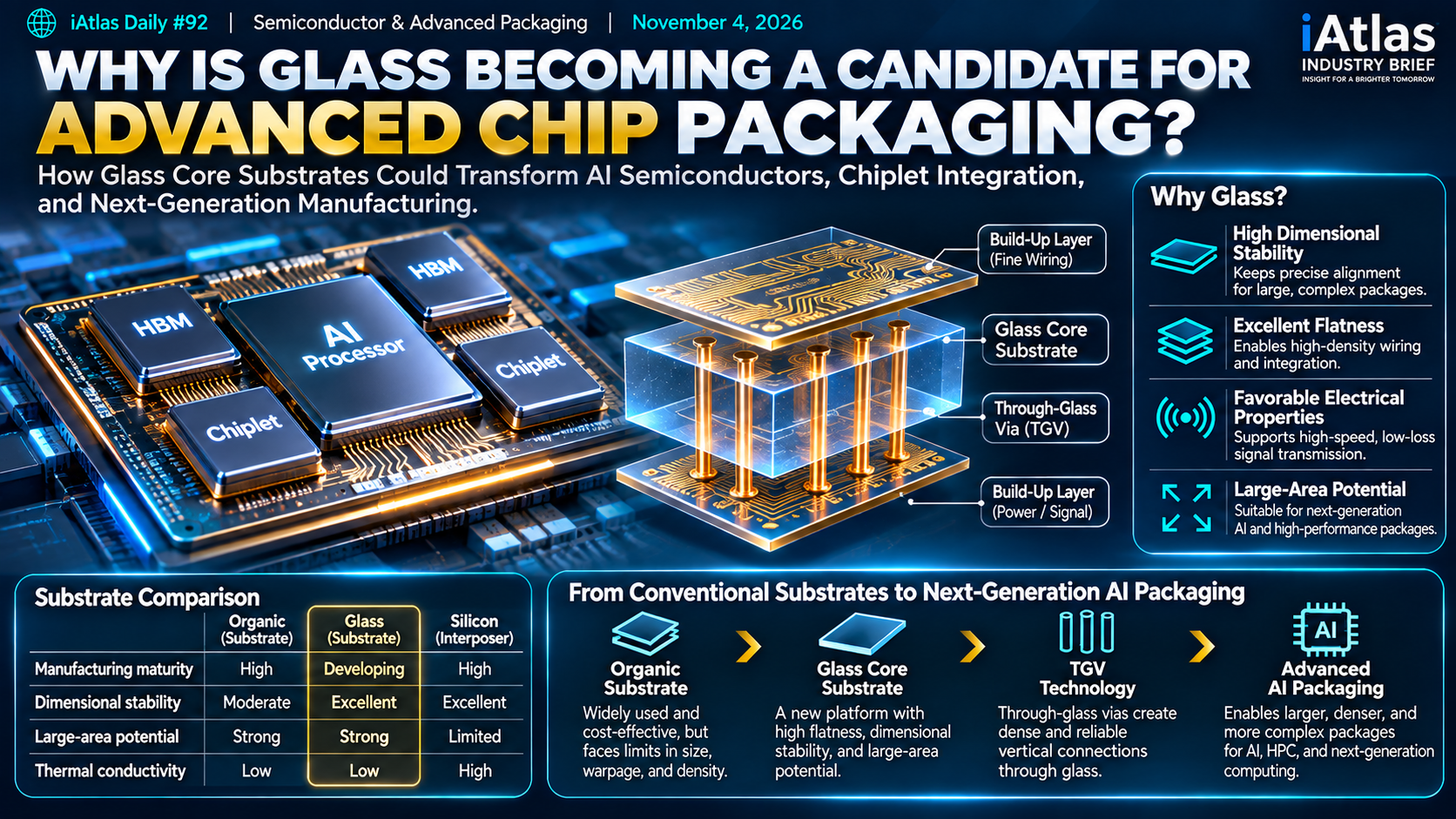
Why Is Glass Becoming a Candidate for Advanced Chip Packaging?
How Glass Core Substrates Could Transform AI Semiconductors, Chiplet Integration, and Next-Generation Manufacturing
iAtlas Daily #92 | Semiconductor & Advanced Packaging | November 4, 2026

The Next Semiconductor Breakthrough May Come From the Material Beneath the Chip
When people think about advanced semiconductors, they usually focus on smaller transistors, faster processors, or more powerful AI chips.
But an important part of the next generation of semiconductor technology may come from something less visible.
The material supporting the chips themselves.
Glass substrates for advanced chip packaging are attracting growing attention as semiconductor manufacturers search for ways to build larger, denser, and more powerful computing systems.
For decades, organic materials have played a central role in semiconductor package substrates.
These materials are widely used, cost-effective, and supported by mature manufacturing processes.
However, advanced AI processors are becoming increasingly complex.
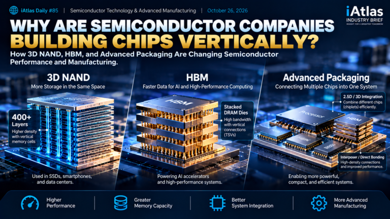
Instead of relying on a single large semiconductor die, manufacturers are combining multiple chiplets, memory devices, and high-speed connections within the same package.
This creates new challenges involving electrical performance, dimensional stability, heat, and manufacturing precision.
Glass is emerging as a potential solution.
Its smooth surface, dimensional stability, and electrical characteristics could support the next generation of high-density semiconductor packaging.
But there is an important distinction.
Glass substrates are not yet a universal replacement for organic substrates. Their future depends on whether manufacturers can solve the challenges of processing fragile materials at industrial scale.
Understanding this technology requires looking beyond the glass itself.
The real story is about how semiconductor packaging is evolving—and why materials that once seemed secondary are becoming strategically important.
1. What Is a Semiconductor Package Substrate?
A semiconductor chip cannot normally operate as a standalone piece of silicon.
It must be electrically connected to other components, supplied with power, protected from environmental damage, and integrated into a larger electronic system.
Semiconductor packaging provides these functions.
One of its essential components is the package substrate.
What Does the Substrate Do?
The package substrate acts as an electrical and mechanical connection platform between semiconductor devices and the larger circuit board.
It performs several functions:
- Supports semiconductor dies
- Distributes electrical power
- Routes electrical signals
- Connects chips to external components
- Provides mechanical support
- Helps manage package reliability
In simplified terms, the substrate is the foundation that allows a semiconductor chip to communicate with the outside world.
Why Is the Substrate Becoming More Important?
Traditional semiconductor packages often contained a relatively simple arrangement of components.
Modern high-performance packages can contain multiple semiconductor dies, advanced memory, and thousands of high-density electrical connections.
As these systems become larger and more complex, the substrate must support increasingly demanding requirements.
A small change in substrate dimensions can affect alignment between components.
Electrical losses can influence signal quality.
Mechanical deformation can reduce manufacturing yield.
The package substrate is therefore becoming an important factor in semiconductor performance.
2. Why Is Advanced Packaging Becoming More Important?
For many years, semiconductor progress was strongly associated with transistor miniaturization.
Smaller transistors helped manufacturers improve performance, increase integration, and reduce energy consumption per operation.
However, advanced semiconductor manufacturing has become increasingly expensive and technically difficult.
This has encouraged companies to explore additional ways to improve computing performance.
One important approach is advanced packaging.
What Is Advanced Packaging?
Advanced packaging combines semiconductor components using sophisticated interconnection and integration technologies.
Examples include:
- 2.5D packaging
- 3D stacking
- Chiplet integration
- Advanced interposers
- High-density redistribution layers
- Heterogeneous integration
These technologies allow manufacturers to combine different semiconductor functions within a single package.
Why Are Chiplets Important?
A chiplet is a smaller semiconductor die designed to perform a particular function.
Instead of manufacturing one extremely large chip, engineers can combine multiple chiplets.
For example, a high-performance computing package may contain:
- Processing chiplets
- Input/output chiplets
- High-bandwidth memory
- Specialized accelerators
- Advanced interconnect structures
This approach offers potential advantages in design flexibility, manufacturing economics, and system integration.
However, connecting multiple chiplets creates a new problem.
The package must support extremely dense electrical connections while maintaining mechanical and thermal reliability.
As semiconductor systems become more complex, the package substrate becomes part of the performance challenge—not merely a supporting component.
3. Why Are Traditional Organic Substrates Facing New Challenges?
Organic package substrates are widely used throughout the semiconductor industry.
Many advanced packages rely on organic build-up materials, including ABF-based substrate technologies.
These materials have supported decades of semiconductor development.
They remain essential to modern computing systems.
But increasingly large packages create additional challenges.
Warpage
Warpage occurs when a substrate bends or deforms.
This can happen because different materials expand and contract at different rates during heating and cooling.
Semiconductor packaging involves multiple thermal processing steps.
When a substrate becomes larger, controlling deformation becomes more difficult.
Excessive warpage can affect alignment, bonding, and manufacturing yield.
Dimensional Stability
High-density semiconductor packaging requires precise alignment between electrical connections.
If a substrate changes dimensions during manufacturing, fine-pitch connections become harder to produce reliably.
Interconnect Density
As more chiplets and memory devices are integrated into one package, manufacturers need additional electrical connections.
This creates demand for finer wiring patterns and more advanced substrate structures.
Larger Package Sizes
AI accelerators and high-performance computing systems are pushing the development of larger semiconductor packages.
Large substrates must remain sufficiently flat and stable throughout assembly.
Organic substrates can continue to improve, but manufacturers are also investigating alternative materials.
Glass is one of the leading candidates.
4. What Makes Glass Attractive for Semiconductor Packaging?
Glass has several properties that may help address advanced packaging challenges.
However, these advantages depend on the glass composition, substrate design, and manufacturing process.
High Dimensional Stability
Glass can provide strong dimensional stability under controlled processing conditions.
This helps maintain alignment during high-precision manufacturing.
Excellent Surface Flatness
Glass can be manufactured with very smooth, flat surfaces.
Flatness is important when forming fine electrical patterns and assembling multiple semiconductor components.
Adjustable Thermal Expansion
Different glass compositions can be engineered to provide different coefficients of thermal expansion.
This may help manufacturers manage mechanical stress between the substrate and other package materials.
Favorable Electrical Properties
Suitable glass compositions can offer low dielectric loss and useful high-frequency electrical characteristics.
This can support signal transmission in advanced computing systems.
Large-Area Manufacturing Potential
Glass processing technologies have already been developed for large-area applications such as displays.
Some of this manufacturing expertise may be relevant to semiconductor substrates.
However, semiconductor packaging imposes different requirements for defects, metallization, interconnections, and reliability.
Higher Processing Temperature Capability
Certain glass materials can tolerate processing conditions that would be difficult for some organic substrate materials.
This may provide additional flexibility in manufacturing and integration.
The Main Advantage
Glass offers a potentially valuable combination of flatness, dimensional stability, and electrical performance.
These properties are especially attractive for large semiconductor packages containing multiple high-performance devices.
But glass also has weaknesses.
It is brittle, and its thermal conductivity is generally much lower than that of silicon.
Its advantages must therefore be evaluated as part of the complete package design.
5. Glass vs. Organic vs. Silicon: What Is the Difference?
Three material platforms are particularly relevant to advanced packaging.
Each has different strengths.
| Characteristic | Organic Substrate | Glass Substrate | Silicon Interposer |
|---|---|---|---|
| Manufacturing maturity | High | Developing | High in established applications |
| Large-area potential | Strong | Strong potential | More constrained by wafer processing |
| Dimensional stability | Requires careful control | Potentially excellent | Excellent |
| Fine interconnections | Advanced processes available | Promising, under development | Extremely fine wiring possible |
| Electrical characteristics | Material-dependent | Favorable for suitable glass | Design-dependent |
| Thermal conductivity | Generally low | Generally low | Relatively high |
| Mechanical challenges | Warpage and expansion | Brittleness and edge damage | Fragility, cost, size constraints |
| Main advantage | Mature supply chain | Flatness and large-area potential | Very fine interconnect technology |
This is a qualitative comparison. Actual performance depends on material composition, substrate architecture, and process technology.
Will Glass Replace Silicon Interposers?
Not necessarily.
A silicon interposer and a glass-core package substrate can perform different functions.
Some advanced package designs may continue to use silicon interposers while adopting new substrate materials elsewhere in the package.
Glass interposers are also being researched.
The semiconductor industry may therefore develop several packaging architectures rather than selecting one universal material.
6. What Is a Glass Core Substrate?
A glass core substrate uses glass as the central structural material of a semiconductor package substrate.
It is not simply an ordinary sheet of glass placed beneath a chip.
The glass core must be integrated with electrical connections, metal layers, insulating materials, and other packaging structures.
A Simplified Structure
A glass-core package substrate may contain:
Semiconductor Dies
The processors, memory devices, or other semiconductor components mounted above the substrate.
Build-Up Layers
Fine electrical wiring and insulating layers used to distribute signals and power.
Glass Core
The central structural layer that provides mechanical support and dimensional stability.
Through-Glass Vias
Vertical electrical connections that pass through the glass core.
External Connections
Structures that connect the package to a circuit board or other electronic assembly.
The glass core serves as the foundation for a complex electrical system.
The challenge is manufacturing all these structures with sufficient precision and reliability.
7. What Are Through-Glass Vias (TGVs)?
One of the most important technologies in glass substrate manufacturing is the through-glass via.
A through-glass via, or TGV, is a small opening that passes through a glass substrate.
When properly metallized, it provides an electrical connection between different sides of the glass.
Why Are TGVs Necessary?
Glass is an electrical insulator.
It does not conduct electricity in the same way as copper or other metals.
To create vertical electrical connections, manufacturers must form holes through the glass and integrate conductive materials.
How Are TGVs Manufactured?
A simplified process may involve:
- Preparing and cleaning the glass substrate
- Forming microscopic holes through the glass
- Preparing the hole surfaces for metallization
- Depositing conductive layers
- Filling or lining the vias with metal
- Forming additional electrical wiring
- Inspecting the completed structures
Different manufacturers may use different process sequences.
How Are the Holes Formed?
Potential techniques include laser-based processing and chemical etching.
Some approaches combine laser modification with selective etching.
The objective is to produce precise openings while minimizing cracks and other defects.
Why Is Metallization Difficult?
A metal conductor must form a reliable electrical connection through the glass.
Manufacturers must control adhesion, voids, uniformity, electrical resistance, and mechanical stress.
Poor metallization can lead to electrical failures or reliability problems.
TGV manufacturing is one of the technologies that will determine whether glass substrates can be produced economically at large scale.
8. Why Is Manufacturing Glass Substrates So Difficult?
Glass offers attractive material properties, but semiconductor manufacturing demands extremely high precision.
Several challenges remain.
Challenge 1 — Brittleness
Glass can crack or chip when subjected to mechanical stress.
Damage may occur during cutting, drilling, handling, or assembly.
Manufacturers need processes that reduce mechanical damage and control defects.
Challenge 2 — Edge Strength
Small defects along the edges of glass panels can reduce mechanical strength.
Edge finishing and inspection are therefore important.
Challenge 3 — Via Formation
Producing large numbers of microscopic holes requires precise control.
Hole geometry, spacing, defects, and process consistency can influence yield.
Challenge 4 — Metal Adhesion
Glass and metals have different material properties.
Creating reliable metal structures on glass requires appropriate surface preparation and metallization technology.
Challenge 5 — Thermal Stress
Different materials expand at different rates when temperatures change.
Glass, copper, semiconductor dies, and insulating materials must work together throughout the package’s operating life.
Challenge 6 — Handling and Automation
Semiconductor manufacturing equipment must transport and process glass without causing damage.
Existing production systems may require modifications.
Challenge 7 — Inspection and Yield
A substrate containing many fine electrical connections must meet strict quality requirements.
Defects in large-area substrates can create significant manufacturing losses.
The challenge is not simply producing one successful prototype.
It is producing thousands of reliable substrates with consistent performance and acceptable cost.
9. Why Is Glass Particularly Interesting for AI Semiconductors?
AI processors are among the most demanding applications for advanced packaging.
They often require high computing performance, substantial memory bandwidth, and efficient power delivery.
Larger Computing Packages
Advanced AI systems increasingly integrate multiple semiconductor devices within the same package.
As the number of components increases, package dimensions and interconnection requirements can grow.
Glass may help support larger substrate formats while maintaining dimensional stability.
High-Density Electrical Connections
Fast communication between semiconductor components requires sophisticated electrical interconnections.
Glass-core technologies could support more demanding wiring structures.
Signal Integrity
High-speed electrical signals can be affected by losses and interference.
Suitable glass materials may provide advantages for certain signal-routing applications.
However, performance depends on the complete interconnect structure—not just the core material.
Power Delivery
Advanced processors require stable electrical power.
Package substrates play an important role in distributing that power.
Glass-based packaging architectures may create opportunities for new power-delivery structures and integrated passive components.
Integration With Optical Technologies
Researchers are also investigating glass for advanced optical and electronic integration.
This could become relevant as computing systems require faster communication between processors and other components.
However, commercial deployment depends on manufacturing readiness and system-level economics.
Glass is attractive because AI packaging requires improvements in several areas at once: size, wiring density, electrical performance, and manufacturing stability.
10. Which Companies Are Developing Glass Substrate Technology?
The glass substrate industry is developing through partnerships between semiconductor companies, substrate manufacturers, materials suppliers, and equipment providers.
Several publicly disclosed initiatives illustrate the direction of the market.
Intel — Early Research and Advanced Packaging Development
In September 2023, Intel announced progress in glass substrate technology for advanced semiconductor packaging.
The company emphasized dimensional stability, package scaling, and higher interconnection density.
Intel described the technology as a potential platform for future high-performance computing systems.
Its announcement highlighted the possibility of significantly improving interconnect density compared with existing substrate approaches.
However, such figures represent technology potential rather than guaranteed performance across commercial products.
Samsung Electro-Mechanics — Glass Core Substrate Development
Samsung Electro-Mechanics has been developing glass-core package substrates for high-performance semiconductor applications.
In January 2025, the company announced that it had established a pilot line at its Sejong facility.
It identified AI accelerators and server processors as potential applications.
In November 2025, Samsung Electro-Mechanics also announced a memorandum of understanding with Sumitomo Chemical Group concerning a joint venture for glass-core manufacturing.
The initiative demonstrates the importance of combining substrate manufacturing expertise with advanced materials technology.
As of October 2026, reported development activities included customer qualification and package-level reliability testing.
Commercial production plans remain subject to customer approval, manufacturing readiness, and project execution.
The Broader Ecosystem
The emerging supply chain includes companies specializing in:
- Specialty glass
- Laser processing
- Precision drilling
- Chemical etching
- Metallization
- Fine-line patterning
- Substrate handling
- Inspection and metrology
- Semiconductor packaging equipment
Glass substrate commercialization will depend on progress across this ecosystem.
A successful glass material alone is not sufficient.
11. What Is the Market Outlook for Glass Core Substrates?
Interest in glass substrates is growing as AI and high-performance computing increase demand for advanced packaging.
In May 2026, SEMI announced a research report examining glass core substrate market development.
The report projected a compound annual growth rate of approximately 67.2% from 2028 to 2040.
This is a long-term market projection for an emerging technology.
It should not be interpreted as evidence that glass substrates are already being adopted across the semiconductor industry.
Why Can Growth Rates Be Misleading?
Emerging markets can produce very high percentage growth rates when starting from a small commercial base.
A rapid growth forecast does not automatically indicate large near-term revenue.
Investors and industry participants should distinguish between:
- Research and development
- Pilot production
- Customer qualification
- Initial commercial production
- High-volume manufacturing
- Broad market adoption
Each stage represents a different level of technical and commercial maturity.
What Will Determine Adoption?
The key factors include manufacturing yield, reliability, total package cost, customer qualification, and the performance advantages of glass compared with existing alternatives.
The market may initially concentrate on applications where performance requirements justify higher costs.
High-performance AI processors and advanced server products are among the potential early application areas.
12. What Could Change by 2030?
The next several years will be important for determining the commercial role of glass substrates.
Three broad scenarios are possible.
Scenario A — Successful Adoption in High-End Packaging
Manufacturers improve TGV processing, metallization, and substrate handling.
Glass-core substrates achieve sufficient yield and reliability for selected high-performance computing products.
Commercial adoption expands gradually.
Scenario B — Selective Adoption Alongside Organic Substrates
Glass finds applications in certain large or demanding packages.
Organic substrates continue to dominate many mainstream semiconductor products.
Different packaging technologies coexist.
Scenario C — Commercialization Takes Longer
Manufacturing costs, reliability challenges, or customer qualification requirements delay broader adoption.
Glass remains important in research and specialized applications while organic substrate technology continues to improve.
These scenarios are not mutually exclusive across the entire industry.
Different manufacturers and product categories may adopt glass at different speeds.
The most realistic expectation is that commercialization will depend on application-specific economics rather than a sudden industry-wide replacement of organic substrates.
Industry Implications | Advanced Packaging Is Becoming a Materials Industry
The development of glass substrates could create opportunities across multiple sectors.
| Industry | Potential Role | Main Challenge |
|---|---|---|
| Specialty Glass | High-performance glass core materials | Consistency, defects, material properties |
| Semiconductor Substrates | Glass-core package manufacturing | Yield, cost, reliability |
| Laser Equipment | Precision via formation | Processing speed, damage control |
| Chemical Processing | Etching, cleaning, surface treatment | Uniformity, chemical compatibility |
| Metallization Equipment | Conductive via and wiring formation | Adhesion, voids, electrical performance |
| Inspection & Metrology | Defect detection and dimensional measurement | Precision, throughput |
| Semiconductor Packaging | Chiplet integration and assembly | Alignment, warpage, reliability |
| AI Computing | Larger and more advanced processor packages | Performance and total system cost |
The opportunity extends beyond glass suppliers.
Specialized equipment manufacturers and chemical process companies may also benefit if commercial production expands.
However, new technology adoption can require substantial capital investment.
Equipment qualification, customer requirements, and production economics will determine which suppliers gain commercial traction.
iAtlas Insight | The Future of Semiconductors May Depend on What Holds the Chips Together
The semiconductor industry has spent decades improving the performance of individual transistors.
That progress remains important.
But the next generation of computing systems increasingly depends on connecting multiple semiconductor devices into larger, more capable packages.
This changes the importance of materials.
A substrate that once appeared to be a supporting component can influence package dimensions, electrical connections, reliability, and manufacturing cost.
Glass illustrates this shift.
Its value does not come from replacing silicon transistors.
Instead, it could help semiconductor manufacturers build more complex systems around those transistors.
Three lessons stand out.
1. Semiconductor Innovation Is Moving Beyond the Chip
Advanced packaging is becoming an important source of performance improvement.
The materials and structures connecting semiconductor devices matter more as integration becomes increasingly complex.
2. Manufacturing Technology Will Determine Commercial Success
Glass offers attractive physical properties.
But its commercial future depends on reliable via formation, metallization, handling, inspection, and assembly.
A material advantage must translate into manufacturing performance.
3. New Materials Create New Supply Chains
Glass substrate adoption could expand opportunities for specialty glass producers, equipment suppliers, chemical processors, and precision manufacturing companies.
The semiconductor supply chain may become more diverse as packaging technologies evolve.
The larger conclusion is that the future of computing will not be determined by transistor scaling alone.
As semiconductor packages become larger and more complex, the material beneath the chips may become just as strategically important as the chips themselves.
Related Articles
Semiconductor Manufacturing
How Thin Film Deposition Builds Semiconductor Devices Layer by Layer
Understand how thin-film processes enable the precise material structures used in semiconductor manufacturing.
Industrial Infrastructure
What Is Industrial Infrastructure?
Explore the facilities, utilities, environmental controls, and equipment systems that support advanced industrial manufacturing.
Industrial Supply Chains
Why Industrial Supply Chain Competition Is Moving Upstream
Discover why specialized materials and manufacturing capabilities are becoming critical sources of industrial competitiveness.
References
Intel’s explanation of glass substrate advantages, package scaling, and high-density semiconductor interconnections.
2. Samsung Electro-Mechanics — CES 2025 CEO Press Meeting (January 2025)
Official announcement covering glass substrate development, pilot manufacturing, and intended applications.
3. Samsung Electro-Mechanics — Glass Core Joint Venture MOU (November 2025)
Official announcement of cooperation with Sumitomo Chemical Group to develop glass-core materials and manufacturing capacity.
4. IEEE Electronics Packaging Society — Glass Core Substrate (January 2026)
Technical discussion of substrate material properties, through-glass via formation, and metallization.
5. SEMI — Glass Core Substrate Market and Development Trends (May 2026)
Industry research announcement covering glass-core market development and advanced packaging demand.
6. Samsung Electro-Mechanics — KPCA Show 2026
Official update on glass substrate technologies, precision processing, and applications in AI and server packaging.
ℹ️ About iAtlas
iAtlas is an independent publication covering batteries, semiconductors, OLED, advanced materials, AI, and global industrial trends.
We transform complex industrial developments into clear, reliable, and easy-to-understand insights.
Whether you’re following today’s industry news or building long-term expertise, iAtlas helps you understand not only what happened, but why it matters.
Technology creates change.
Insight creates opportunity.
— iAtlas