Why HBM Is Redefining AI Computing
The Memory Technology Behind the AI Revolution
📰 iAtlas Daily #5 | July 7, 2026
Today’s Highlights
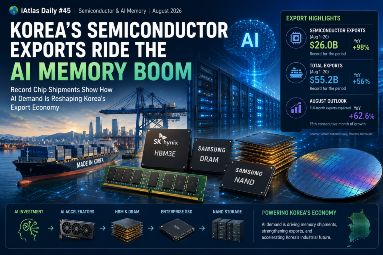
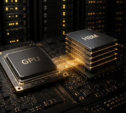
- AI processors are becoming increasingly dependent on High Bandwidth Memory (HBM).
- Faster memory is now just as important as faster GPUs.
- The rapid growth of AI is accelerating innovation in memory packaging and advanced semiconductor manufacturing.
Cover Story
AI Needs More Than Powerful GPUs
When people talk about AI hardware, they often focus on GPUs.
However, even the world’s most powerful processor cannot perform efficiently without fast memory.
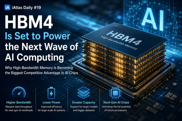
This is where High Bandwidth Memory (HBM) has become one of the most critical technologies in modern computing.
HBM dramatically increases the speed at which processors access data, enabling today’s AI models to train and run efficiently.
As AI workloads continue to grow, memory performance is becoming just as important as computing performance.
AI Computing

Why Traditional Memory Is No Longer Enough
Conventional DRAM has served the computing industry for decades.
But modern AI models process enormous amounts of data simultaneously.
To keep GPUs operating efficiently, memory must deliver:
- Extremely high bandwidth
- Low power consumption
- Short signal paths
- Massive parallel data transfer
HBM was specifically designed to meet these demands.
Semiconductor
Stacking Memory for Performance
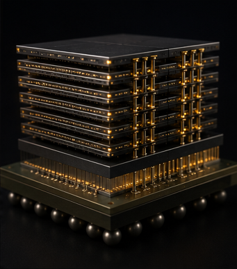
Unlike traditional memory chips placed separately on a circuit board, HBM stacks multiple memory dies vertically.
These layers are connected using Through-Silicon Vias (TSVs), allowing data to move much faster while reducing power consumption.
HBM packages are then integrated closely with AI processors using advanced packaging technologies.
This combination delivers exceptional computing performance for AI applications.
Manufacturing
Packaging Is Becoming the Key Technology
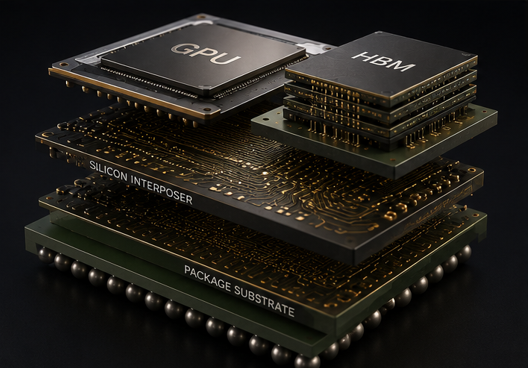
Modern AI chips are no longer built around a single processor.
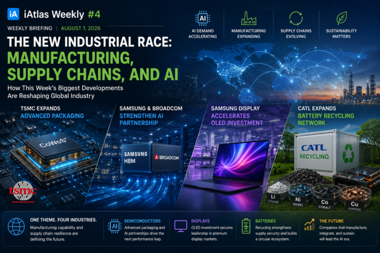
Instead, GPUs, HBM memory, and chiplets are assembled together using advanced packaging platforms.
This makes technologies such as:
- Glass Substrate
- Silicon Interposer
- Chiplet Integration
- Advanced Packaging
more important than ever before.
The future of AI computing depends not only on faster chips but also on better integration.
🎯 Atlas Radar
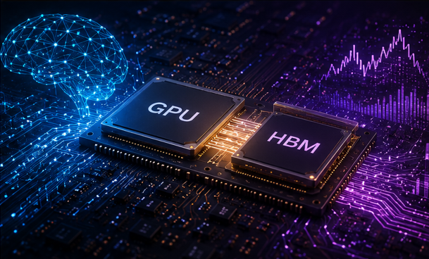
What Is HBM?
High Bandwidth Memory is a next-generation memory architecture that stacks multiple DRAM dies vertically to maximize bandwidth while minimizing power consumption.
Why It Matters
Without HBM, today’s large AI models would struggle to achieve the performance required for training and inference.
HBM has become one of the essential building blocks of modern AI infrastructure.
🔭 Atlas Outlook
Looking Ahead
HBM Demand Will Continue Growing
As AI models become larger and more complex, demand for HBM is expected to increase significantly.
Packaging Innovation Will Accelerate
The need to integrate GPUs and HBM more efficiently will continue driving innovation in semiconductor packaging.
Memory Will Become a Competitive Advantage
Future AI leadership will depend not only on processor design but also on memory technology.
💡 Atlas Insight
The AI race is no longer just about faster processors.
It is increasingly about how quickly those processors can access data.
HBM has transformed memory from a supporting component into a core driver of AI performance.
Understanding AI hardware means understanding memory.
Today’s Keywords
High Bandwidth Memory (HBM)
A next-generation memory technology designed to provide extremely high data bandwidth for AI and high-performance computing.
TSV (Through-Silicon Via)
Vertical electrical connections that enable stacked memory dies to communicate at very high speeds.
Advanced Packaging
Technologies that integrate processors, memory, and chiplets into a single high-performance package.
📚 Continue Reading
Previous Daily
➡️ Why Glass Substrate Could Replace Today’s Chip Packaging
Discover why glass substrates are emerging as one of the most important innovations in advanced semiconductor packaging.
→ Read Daily 4
Also Recommended
➡️ Why 300mm Wafers Matter for AR/VR
Explore how larger silicon wafers are transforming Micro OLED manufacturing for next-generation AR and VR devices.
Coming Next
➡️ Inside OLED Material Purification
Why high-purity OLED materials are becoming essential for next-generation display manufacturing.
Coming Soon
About iAtlas
iAtlas is an independent industry publication covering batteries, semiconductors, OLED, advanced materials, and emerging technologies.
We explain not only what is happening, but why it matters.
Technology creates change.
Insight creates opportunity.
— iAtlas