Silicon Wafer Manufacturing: Cutting, Lapping, and Polishing Explained
💻 iAtlas Semiconductor #4 | 📘 Fundamentals → Wafer Manufacturing
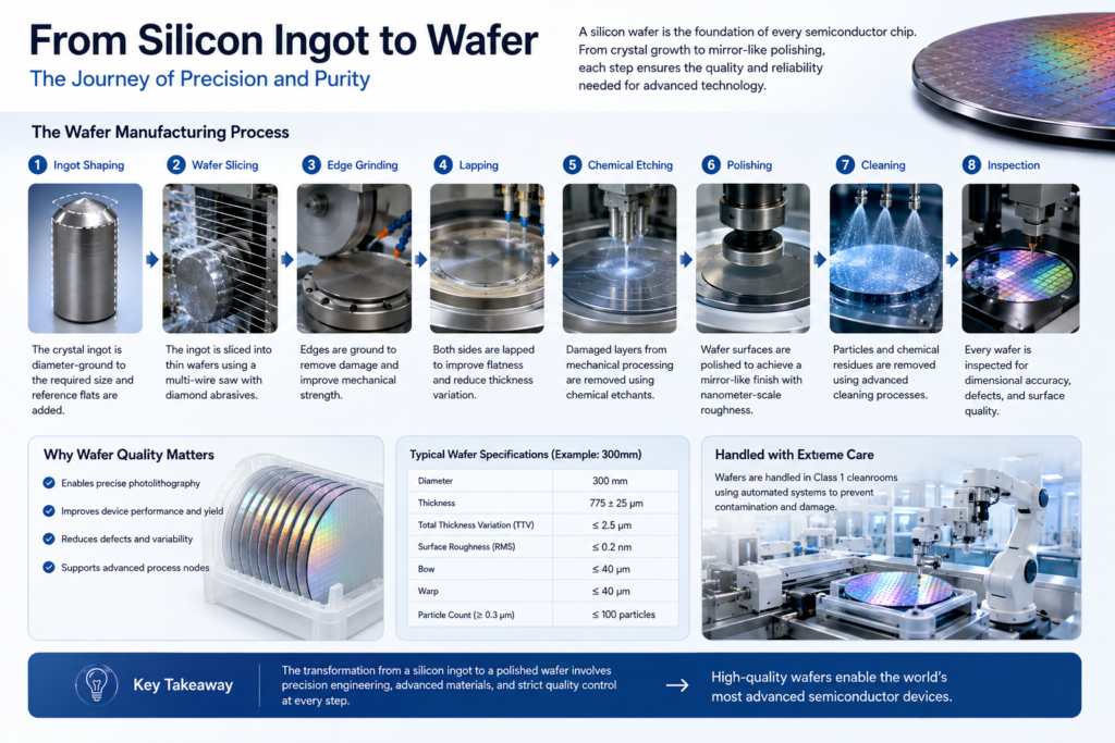
Introduction
Silicon wafer manufacturing begins after the Czochralski Process produces a single-crystal silicon ingot.
Before integrated circuits can be built, the ingot must be transformed into ultra-flat, mirror-like silicon wafers with extremely tight dimensional tolerances.
This transformation involves several precision manufacturing processes, including slicing, edge shaping, lapping, chemical etching, polishing, cleaning, and inspection.
Although these steps receive less attention than photolithography or chip design, they play a critical role in determining wafer quality and manufacturing yield.
Why Wafer Manufacturing Matters
A semiconductor wafer serves as the foundation for hundreds of fabrication steps.
If the wafer surface is not perfectly flat, later processes such as lithography, thin-film deposition, and etching become increasingly difficult to control.
Modern semiconductor manufacturing therefore demands wafers with:
- Extremely low surface roughness
- Excellent flatness
- Minimal thickness variation
- Very low particle contamination
- High mechanical strength
Every polishing and cleaning step contributes to achieving these requirements.
From Crystal to Wafer
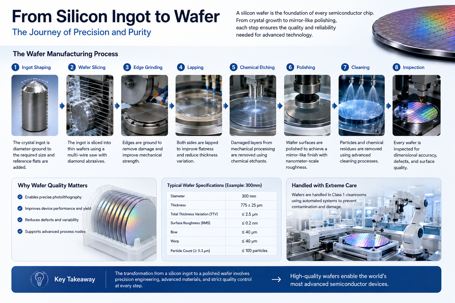
Once crystal growth is complete, the silicon ingot passes through a series of precision manufacturing processes.
The simplified flow is:
- Ingot Shaping
- Wafer Slicing
- Edge Grinding
- Lapping
- Chemical Etching
- Polishing
- Cleaning
- Inspection
Each step improves the dimensional accuracy and surface quality of the wafer before it enters semiconductor fabrication.
Step 1. Ingot Shaping
The crystal grown by the Czochralski Process is first machined into the required diameter.
Small reference features may also be added to identify crystal orientation and wafer type.
Modern 300 mm wafers rely on extremely accurate diameter control to ensure compatibility with automated manufacturing equipment.
Step 2. Wafer Slicing
The cylindrical ingot is cut into thin discs using a multi-wire saw.
Instead of using a traditional blade, modern slicing systems employ hundreds of fine steel wires coated with abrasive particles.
This method provides:
- High dimensional accuracy
- Reduced material loss
- Better surface consistency
- Improved productivity
Despite its precision, slicing leaves microscopic damage and saw marks on the wafer surface.
Step 3. Edge Grinding
Freshly sliced wafers have sharp edges that are susceptible to chipping and cracking.
Edge grinding rounds the wafer perimeter to improve mechanical strength and reduce the risk of damage during handling.
This step also enhances wafer durability throughout the many process stages that follow.
Step 4. Lapping
After slicing, the wafer surfaces are not perfectly flat.
Lapping removes damaged material while improving thickness uniformity.
During this process, abrasive slurry and precision equipment gradually smooth both wafer surfaces.
Lapping helps reduce:
- Saw damage
- Thickness variation
- Surface waviness
Step 5. Chemical Etching
Mechanical processing introduces a thin layer of damaged silicon beneath the surface.
Chemical etching removes this damaged layer using carefully controlled chemical reactions.
This improves crystal quality near the surface and prepares the wafer for polishing.
Step 6. Polishing
Polishing creates the mirror-like surface required for semiconductor manufacturing.
Modern polishing techniques achieve nanometer-scale surface roughness.
The resulting surface allows photolithography systems to accurately focus light and transfer circuit patterns with extremely high precision.
Without this level of flatness, advanced semiconductor manufacturing would not be possible.
Step 7. Cleaning
Particles, metals, organic residues, and polishing chemicals must all be removed before fabrication begins.
Wafer cleaning uses multiple chemical cleaning steps and ultrapure water to eliminate contaminants.
The goal is to deliver wafers with virtually no surface contamination.
Step 8. Inspection
Every finished wafer undergoes extensive quality inspection.
Key measurements include:
- Diameter
- Thickness
- Total Thickness Variation (TTV)
- Surface Flatness
- Bow
- Warp
- Particle Count
- Surface Defects
Only wafers meeting strict specifications proceed to semiconductor fabrication facilities.
Mirror-Like Surfaces Matter
At first glance, a polished silicon wafer looks like a perfectly smooth mirror.
In reality, its surface quality is controlled at the nanometer level.
This precision ensures that later processes such as:
- Photolithography
- Thin Film Deposition
- Plasma Etching
- Chemical Mechanical Planarization (CMP)
can be performed consistently across the entire wafer.
Automation and Wafer Handling
Modern wafer manufacturing is highly automated.
Because even microscopic particles can damage future semiconductor devices, wafers are handled using:
- FOUPs (Front Opening Unified Pods)
- Robotic transfer systems
- Edge-grip handling mechanisms
- Class 1 cleanrooms
Human contact with the wafer surface is avoided throughout production.
Looking Ahead
As semiconductor manufacturing advances, wafer requirements continue to become more demanding.
Future developments include:
- Lower Total Thickness Variation (TTV)
- Reduced surface roughness
- Larger wafer diameters
- Engineered substrates
- Improved automation
- Higher manufacturing productivity
These improvements help support next-generation semiconductor technologies, including advanced packaging, 3D integration, and AI processors.
Key Takeaways
- Silicon ingots must undergo multiple precision processes before becoming semiconductor wafers.
- Wafer slicing, lapping, etching, polishing, cleaning, and inspection all contribute to wafer quality.
- Surface flatness and cleanliness are essential for successful semiconductor fabrication.
- Modern wafer manufacturing relies heavily on automation and nanometer-level precision.
Frequently Asked Questions
What is wafer manufacturing?
Wafer manufacturing transforms a single-crystal silicon ingot into a precision semiconductor wafer through slicing, lapping, polishing, cleaning, and inspection.
Why is wafer polishing important?
Polishing creates the mirror-like surface required for accurate photolithography and nanometer-scale semiconductor fabrication.
What is TTV in wafer manufacturing?
Total Thickness Variation (TTV) measures thickness uniformity across a wafer and directly affects process accuracy.
📖 Semiconductor Learning Path
Previous
💻 Semiconductor #1 | What Is Semiconductor Manufacturing?
💻 Semiconductor #2 | Why Silicon Wafers Are the Foundation of Modern Chips
💻 Semiconductor #3 | How the Czochralski Process Creates Single-Crystal Silicon
⬇️
Current
💻 Semiconductor #4 | From Silicon Ingot to Wafer: Cutting, Lapping, and Polishing
⬇️
Next
💻 Semiconductor #5 | How Photolithography Creates Microscopic Circuit Patterns
📚 Continue Reading
- 💻 Semiconductor #5 | How Photolithography Creates Microscopic Circuit Patterns
- 💻 Semiconductor #6 | How Plasma Etching Shapes Modern Semiconductor Devices
- 💻 Semiconductor #7 | Thin Film Deposition: Building Semiconductor Layers
- 💻 Semiconductor #8 | Ion Implantation: Engineering Silicon at the Atomic Level
- 💻 Semiconductor #9 | Chemical Mechanical Planarization (CMP) Explained
References
- SEMI
- IEEE Electron Devices Society (EDS)
- Semiconductor Industry Association (SIA)
- SUMCO – Silicon Wafer Manufacturing
- GlobalWafers
- Siltronic
🔷 About iAtlas
iAtlas is an independent publication covering batteries, semiconductors, OLED, advanced materials, AI, and global industrial trends.
We transform complex industrial developments into clear, reliable, and easy-to-understand insights.
Whether you’re following today’s industry news or building long-term expertise, iAtlas helps you understand not only what happened, but why it matters.
Technology creates change.
Insight creates opportunity.
— iAtlas