How the Czochralski Process Creates Single-Crystal Silicon
💻 iAtlas Semiconductor #3 | 📘 Fundamentals → Crystal Growth
Introduction
Every semiconductor chip begins with silicon, but not just any silicon.
Modern integrated circuits require an extremely pure and perfectly ordered crystal structure capable of supporting billions of microscopic transistors. Before a silicon wafer can enter photolithography, etching, or deposition, it must first be grown into a single crystal with exceptional uniformity.
The technology responsible for creating this foundation is the Czochralski (CZ) Process.
Invented over a century ago and continuously refined for modern semiconductor manufacturing, the Czochralski Process remains the world’s most widely used method for producing single-crystal silicon ingots. These ingots are later sliced into wafers that become the starting point for nearly every advanced semiconductor device.
Understanding the CZ Process helps explain why wafer quality directly influences chip performance, manufacturing yield, and the future of semiconductor technology.
Why Single-Crystal Silicon Matters
Silicon atoms naturally arrange themselves in a crystal lattice.
If that lattice is continuous and perfectly aligned, electrons can travel through the material in a predictable way. However, if multiple crystals grow together, boundaries form between them.
These grain boundaries interrupt electrical behavior and create defects that reduce semiconductor performance.
For integrated circuits containing billions of transistors, even tiny crystal imperfections can reduce yield and reliability.
Single-crystal silicon offers several advantages:
- Uniform electrical characteristics
- Lower crystal defect density
- Higher manufacturing yield
- Better transistor performance
- Improved long-term reliability
For these reasons, virtually all advanced logic and memory chips begin with single-crystal silicon rather than polycrystalline material.
What Is the Czochralski Process?
The Czochralski Process is a crystal growth technique used to produce large cylindrical single-crystal silicon ingots.
The method was invented in 1916 by Polish scientist Jan Czochralski. Although originally developed for metals, it later became the standard process for manufacturing semiconductor-grade silicon.
Today, most 200 mm and 300 mm silicon wafers used in advanced semiconductor fabrication originate from CZ-grown crystals.
The basic principle is surprisingly simple:
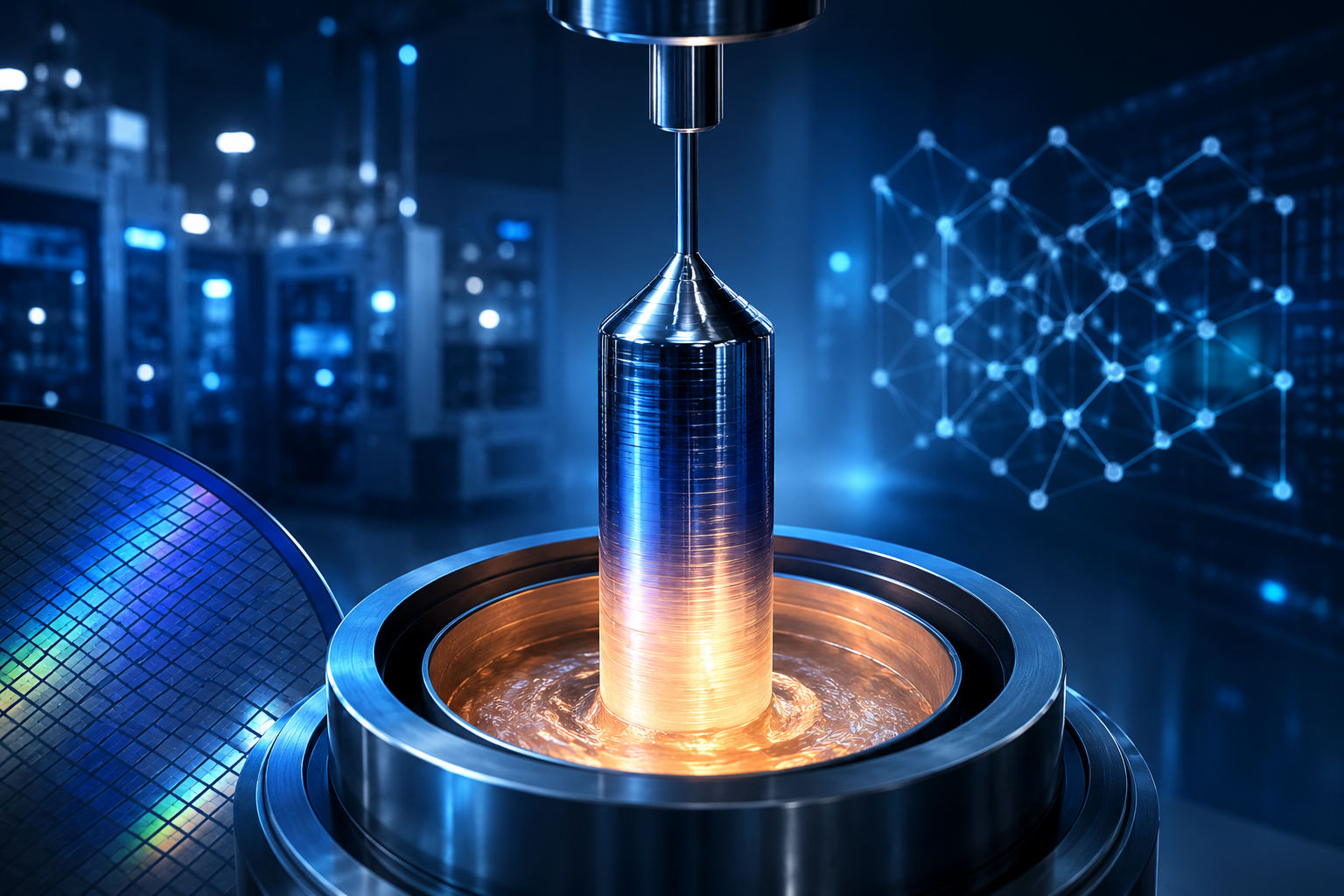
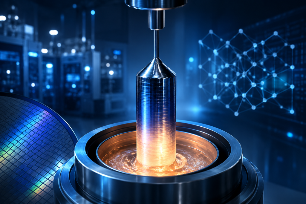
A small single crystal is dipped into molten silicon and then slowly pulled upward while rotating.
As the silicon cools, atoms arrange themselves in exactly the same crystal orientation as the seed crystal, gradually forming one continuous crystal.
Step 1. Producing Ultra-Pure Silicon
The process begins long before crystal growth.
Raw quartz contains silicon, but it also contains many impurities that are unacceptable for semiconductor manufacturing.
Through multiple purification processes, metallurgical-grade silicon is refined into electronic-grade silicon (EGS) with a purity exceeding 99.999999999% (11N purity).
At this level, unwanted impurities exist only at extremely low concentrations, allowing precise control of electrical properties during later manufacturing stages.
Step 2. Melting the Silicon
Electronic-grade silicon is loaded into a high-purity quartz crucible inside a crystal growth furnace.
The furnace heats the silicon above its melting point of approximately 1,420°C, creating a pool of molten silicon.
Throughout this stage, an inert argon atmosphere protects the melt from oxidation and contamination.
Temperature stability is critical because even small fluctuations can affect crystal quality and diameter control.
Step 3. Introducing the Seed Crystal
A small piece of single-crystal silicon known as the seed crystal is lowered until it touches the molten silicon.
The seed determines the crystal orientation of the entire ingot.
Once contact is established, both the seed and the crucible begin rotating.
The seed is then pulled upward at a carefully controlled speed.
As molten silicon cools around the seed, atoms align with its crystal lattice instead of forming random structures.
This produces one continuous crystal that can eventually exceed two meters in length.
Step 4. Growing the Silicon Ingot
Crystal growth is one of the most carefully controlled stages of semiconductor manufacturing.
Several parameters must remain stable throughout the entire process:
- Pulling speed
- Rotation speed
- Furnace temperature
- Thermal gradient
- Melt level
- Crystal diameter
If any of these parameters change unexpectedly, the ingot diameter may fluctuate or crystal defects may form.
Advanced control systems continuously monitor these conditions to maintain consistent crystal quality from top to bottom.
Controlling Ingot Diameter
Modern semiconductor manufacturing relies heavily on standardized wafer sizes.
For advanced production, the industry primarily uses 300 mm wafers.
To achieve this, the crystal must be grown with an extremely consistent diameter over a length of several meters.
If the pulling speed increases too quickly, the crystal diameter becomes smaller.
If cooling occurs too slowly, the crystal may become wider than intended.
Maintaining a stable diameter requires precise control of both heat transfer and crystal growth dynamics throughout the entire process.
Crystal Orientation
Not all silicon crystals are identical.
The orientation of the crystal lattice affects oxidation, etching behavior, carrier mobility, and device performance.
Common crystal orientations include:
- (100) — Widely used for CMOS logic and memory devices
- (111) — Often selected for MEMS and specialized applications
- (110) — Used in certain advanced device structures
The seed crystal determines this orientation, and the entire ingot inherits the same atomic arrangement.
Dopant Control During Crystal Growth
Pure silicon has limited electrical conductivity.
To create semiconductor devices, controlled amounts of dopant atoms are added during crystal growth.
Common dopants include:
| Dopant | Result |
|---|---|
| Boron | P-type silicon |
| Phosphorus | N-type silicon |
| Arsenic | N-type silicon |
| Antimony | N-type silicon |
The concentration of these dopants determines wafer resistivity and influences the electrical characteristics of the final devices.
Maintaining uniform dopant distribution throughout the crystal is essential for consistent semiconductor performance.
The Challenge of Oxygen and Carbon
Although the CZ Process is widely used, it also introduces certain impurities.
Because molten silicon is contained inside a quartz crucible, small amounts of oxygen dissolve into the crystal during growth.
Carbon contamination may also occur through interactions with furnace components.
Excessive oxygen or carbon can influence:
- Crystal defects
- Mechanical strength
- Thermal behavior
- Device reliability
Modern crystal growth systems therefore optimize furnace design and process conditions to minimize unwanted contamination while maintaining stable crystal growth.
CZ Process vs. Float Zone Process
Two major methods are used to produce single-crystal silicon.
| Feature | Czochralski (CZ) | Float Zone (FZ) |
|---|---|---|
| Production volume | High | Low |
| Oxygen content | Higher | Extremely low |
| Typical wafer size | Up to 300 mm | Usually smaller |
| Cost | Lower | Higher |
| Main applications | Logic, memory, consumer electronics | Power devices, high-voltage applications |
Because of its excellent productivity and scalability, the CZ Process remains the dominant technology for mainstream semiconductor manufacturing.
Why Crystal Quality Determines Chip Yield
The quality of the silicon crystal affects every manufacturing step that follows.
Crystal defects may contribute to:
- Pattern distortion
- Electrical leakage
- Reduced carrier mobility
- Localized device failure
- Lower manufacturing yield
Since hundreds of process steps occur after wafer fabrication begins, defects introduced during crystal growth can become extremely expensive later in production.
For this reason, semiconductor manufacturers invest heavily in crystal growth technology before the first wafer is even produced.
The Future of Crystal Growth
As semiconductor devices continue to shrink and advanced packaging becomes more important, crystal growth technology must continue evolving.
Current research focuses on:
- Lower oxygen concentration
- Reduced crystal defects
- Improved diameter uniformity
- Better dopant control
- Higher productivity
- Advanced engineered substrates
- Materials for power semiconductors such as SiC and GaN
Although new semiconductor materials are gaining attention, silicon grown through the Czochralski Process is expected to remain the foundation of mainstream semiconductor manufacturing for many years.
Key Takeaways
- The Czochralski Process is the world’s most widely used method for producing single-crystal silicon.
- Single-crystal silicon provides the uniform electrical properties required for advanced semiconductor devices.
- Crystal growth begins with ultra-pure molten silicon and a precisely controlled seed crystal.
- Diameter, temperature, rotation speed, and pulling speed must all be carefully managed throughout the growth process.
- Dopant concentration and crystal orientation are established during crystal growth and influence later device performance.
- Crystal quality has a direct impact on wafer quality, manufacturing yield, and chip reliability.
- Nearly every modern logic and memory chip begins with a CZ-grown silicon crystal.
📖 Semiconductor Learning Path
Previous
💻 Semiconductor #1 | What Is Semiconductor Manufacturing?
💻 Semiconductor #2 | Why Silicon Wafers Are the Foundation of Modern Chips
Current
💻 Semiconductor #3 | How the Czochralski Process Creates Single-Crystal Silicon
Next
💻 Semiconductor #4 | From Silicon Ingot to Wafer: Cutting, Lapping, and Polishing
📚 Continue Reading
- 💻 Semiconductor #1 | What Is Semiconductor Manufacturing?
- 💻 Semiconductor #2 | Why Silicon Wafers Are the Foundation of Modern Chips
- 💻 Semiconductor #4 | From Silicon Ingot to Wafer: Cutting, Lapping, and Polishing
- 💻 Semiconductor #5 | How Photolithography Creates Microscopic Circuit Patterns
- 💻 Semiconductor #6 | How Plasma Etching Shapes Modern Semiconductor Devices
References
🔷 About iAtlas
iAtlas is an independent publication covering batteries, semiconductors, OLED, advanced materials, AI, and global industrial trends.
We transform complex industrial developments into clear, reliable, and easy-to-understand insights.
Whether you’re following today’s industry news or building long-term expertise, iAtlas helps you understand not only what happened, but why it matters.
Technology creates change.
Insight creates opportunity.
— iAtlas