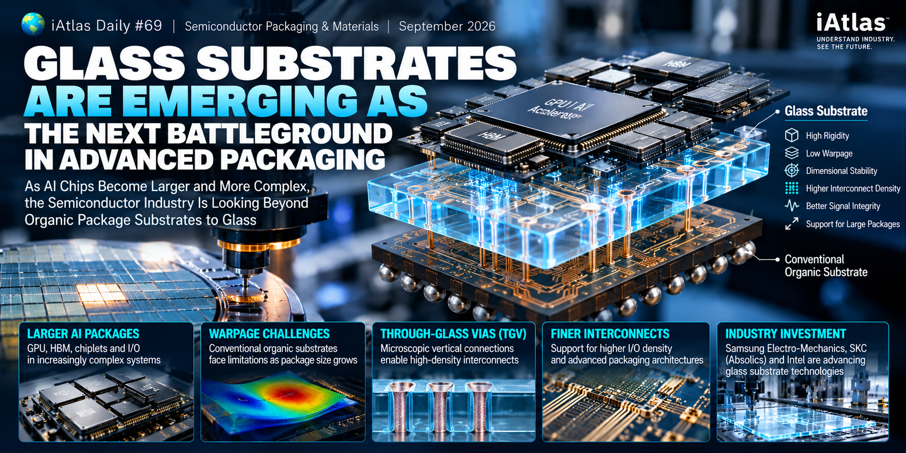
Glass Substrates Are Emerging as the Next Battleground in Advanced Packaging
As AI Chips Become Larger and More Complex, the Semiconductor Industry Is Looking Beyond Organic Package Substrates to Glass
🔲 iAtlas Daily #69 | Semiconductor Packaging & Materials | September 2026
For decades, semiconductor progress was largely associated with one direction:
Smaller Transistors
Smaller transistors allowed more computing power to fit onto a chip.
But AI is changing the physical structure of semiconductor systems.
Modern AI processors increasingly combine:
GPU / Accelerator
HBM
Chiplets
I/O
and:
Advanced Packaging
into increasingly large packages.
As the package becomes larger and more complex, another component becomes increasingly important:
The Substrate
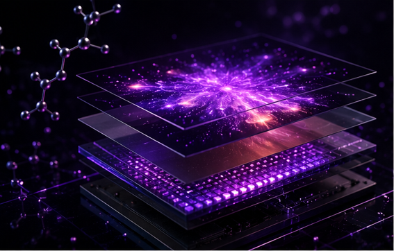
The substrate sits underneath the semiconductor chips.
It provides:
Mechanical Support
Electrical Connections
Power Delivery
and:
Signal Routing
between the chips and the rest of the system.
Traditionally, advanced semiconductor packages have relied heavily on organic substrate materials.
But as packages become:
Larger
Denser
and:
More Power Hungry
the limitations of conventional organic substrates become more difficult to manage.
That is creating an opportunity for another material:
Glass
This month, Samsung Electro-Mechanics showcased its next-generation glass substrate technology at KPCA Show 2026.
SKC is investing hundreds of billions of won into Absolics as the company moves its glass substrates through customer reliability evaluation.
And Intel is working with Lens Technology to develop glass-based advanced packaging solutions.
The semiconductor industry’s next materials transition may therefore happen not inside the transistor—
but:
Underneath the chip.
As semiconductor scaling expands from the transistor into the package, the materials supporting that package are becoming part of the performance equation.
🌍 The Big Story
A semiconductor package may look simple from the outside.
But inside a modern high-performance package, multiple components must communicate at enormous speed.
Consider an AI accelerator.
It may contain:
Compute Dies
HBM Stacks
I/O Components
Power Connections
all inside one package.
These components need to exchange huge amounts of data.
That creates a fundamental manufacturing challenge:
How do you connect more chips across a larger package while maintaining precision, electrical performance and structural stability?
One possible answer is:
Glass Substrate
Glass offers physical and electrical characteristics that could make it particularly suitable for the next generation of large advanced semiconductor packages.
1. What Is a Semiconductor Package Substrate?
The semiconductor die does not normally connect directly to a computer motherboard.
Between them sits a package substrate.
A simplified structure looks like:
Semiconductor Chip
↓
Bumps
↓
Package Substrate
↓
Solder Connections
↓
Mainboard
The substrate distributes:
Electrical Signals
and:
Power
while also supporting the semiconductor mechanically.
For increasingly complex processors, this role becomes much more demanding.
Samsung Electro-Mechanics describes the package substrate as evolving from a simple interconnection component into a technology that directly affects:
Performance
Power Efficiency
and:
Signal Stability. Samsung Semiconductor
2. AI Is Making Semiconductor Packages Larger
Traditional processors could often be designed primarily around a single large die.
But semiconductor architectures are changing.
Instead of:
One Chip
we increasingly see:
Multiple Compute Dies
Memory
Chiplets
integrated together.
This creates:
Larger Package Area
AI accelerators are one of the strongest examples.
They need enormous memory bandwidth.
That is why HBM stacks are placed extremely close to the compute processor.
The package therefore needs to accommodate:
More Components
More Connections
and:
More Power
in a tightly integrated structure.
3. Larger Packages Create a Physical Problem
As substrates become larger, maintaining dimensional stability becomes more difficult.
One major issue is:
Warpage
Warpage means the substrate bends or deforms rather than remaining perfectly flat.
Imagine a thin sheet changing shape slightly during processing.
At everyday scale, a small bend may seem insignificant.
At semiconductor scale, it can create serious problems.
Connections may no longer align correctly.
That can affect:
Bump Alignment
Assembly
Yield
and:
Reliability
The larger the package becomes, the more difficult warpage management can become.
4. Why Do Organic Substrates Warp?
Conventional package substrates typically contain combinations of:
Organic Resin
Copper
and:
Reinforcement Materials
Different materials expand differently when heated.
During semiconductor manufacturing and operation, the package experiences temperature changes.
That creates:
Thermal Expansion
↓
Material Stress
↓
Dimensional Change
↓
Potential Warpage
Manufacturers already use sophisticated engineering to control this.
But as packages become larger, the challenge becomes harder.
5. Glass Has Different Physical Properties
Glass offers several potentially attractive characteristics.
It can provide:
High Rigidity
Excellent Flatness
Dimensional Stability
and:
Low Thermal Expansion
relative to many conventional organic structures.
Samsung Electro-Mechanics specifically highlights the ability of glass substrates to improve rigidity and dimensional stability while supporting better signal and power characteristics. Samsung Semiconductor
This is why glass becomes particularly interesting for:
Large-Area Advanced Packaging
6. Think of It as Building on a Flatter Foundation
A simple analogy helps.
Imagine constructing a very precise structure.
If the foundation moves or bends:
Alignment becomes harder.
But if the foundation remains extremely flat:
More precise structures can be built on top.
The same basic idea applies here.
Glass can potentially provide a more dimensionally stable platform for increasingly complex semiconductor packages.
That can help enable:
Finer Wiring
Higher Interconnect Density
and:
Larger Packages
7. But Glass Alone Does Not Connect Anything
A plain sheet of glass is not a semiconductor substrate.
Electrical signals need to move:
Across
and:
Through
the glass.
This requires one of the most important technologies in glass substrates:
TGV
Through-Glass Via
A TGV is a tiny connection channel formed through the glass.
The simplified process is:
Glass
↓
Create Microscopic Hole
↓
Fill / Plate with Conductive Metal
↓
Create Vertical Electrical Connection
These vias allow signals and power to pass from one side of the glass to the other.
8. TGV Is One of the Key Manufacturing Challenges
Creating one hole in glass is easy.
Creating:
Thousands
or potentially:
Millions
of microscopic structures with consistent:
Diameter
Position
Shape
and:
Electrical Performance
is much harder.
Manufacturing can involve technologies such as:
Laser Processing
Etching
Metallization
Plating
and:
Precision Inspection
Samsung Electro-Mechanics highlighted both fine connection-channel formation and metal filling as core glass-substrate technologies at KPCA Show 2026. Samsung Semiconductor
This is where glass substrate technology becomes a manufacturing challenge rather than simply a materials choice.
9. Glass Can Potentially Enable Finer Interconnects
Modern AI packages need enormous numbers of electrical connections.
As interconnect density increases, wiring needs to become:
Smaller
and:
Closer Together
Glass’s dimensional stability can help support finer circuit structures.
This could enable:
Higher-Density Interconnects
which are increasingly important for connecting:
Compute
↔
Memory
↔
Chiplets
inside advanced packages.
10. Signal Integrity Matters More as Data Rates Increase
Modern AI processors move enormous amounts of data.
HBM exists largely because processors need far more memory bandwidth than conventional memory architectures can provide.
But moving data at very high speed creates electrical challenges.
Signals can experience:
Loss
Interference
Noise
and:
Distortion
Package materials therefore affect more than mechanical structure.
They also influence:
Electrical Performance
Intel’s glass-substrate development work specifically targets higher interconnect density and improved power efficiency for future AI and data-center platforms. Intel
11. Power Delivery Is Becoming Another Packaging Challenge
AI chips consume enormous amounts of power.
That power needs to reach the processors reliably.
As compute density rises:
Power Demand
↑
Current Density
↑
Power-Delivery Complexity
↑
The package substrate plays a role in distributing that power.
This means next-generation substrates need to support both:
High-Speed Data
and:
High-Density Power Delivery
at the same time.
The substrate is therefore becoming part of system-level semiconductor design.
12. Glass Could Also Reduce Layer Count
Traditional organic substrates often require multiple build-up layers to create complex routing structures.
Glass-based architectures may allow some designs to achieve the required connectivity with fewer layers.
Samsung Electro-Mechanics says glass can potentially lower the number of substrate layers while improving signal characteristics and power efficiency. Samsung Semiconductor
Fewer layers could eventually affect:
Thickness
Manufacturing Complexity
and:
Cost
But these benefits depend heavily on whether glass processing itself can become economically competitive.
13. That Is the Critical Question
Glass has attractive engineering properties.
But semiconductor manufacturing is not decided by engineering performance alone.
The technology must also achieve:
High Yield
High Throughput
Low Defectivity
Reliability
and:
Competitive Cost
This is where the glass-substrate race becomes much more difficult.
14. Glass Is Also Fragile
The same material that provides excellent dimensional stability creates another challenge.
Glass can:
Crack
or:
Break
That creates difficulties during:
Handling
Drilling
Dicing
Transport
and:
Assembly
The manufacturing system therefore needs to control:
Mechanical Stress
and:
Edge Damage
very carefully.
Replacing organic material with glass does not eliminate manufacturing problems.
It exchanges one set of problems for another.
15. This Is Why Commercialization Has Taken Time
Glass substrates have been discussed for several years.
Yet they are still not widely used in mainstream commercial semiconductor packages.
Why?
Because a promising material must survive the entire manufacturing sequence.
The commercialization path looks like:
Material Development
↓
Prototype
↓
Process Development
↓
Reliability Testing
↓
Customer Qualification
↓
Yield Improvement
↓
Mass Production
Glass substrates are now moving through the later parts of this sequence.
But they have not completed it.
16. Absolics Is One of the Companies Closest to Commercialization
One of the most important companies in this field is:
Absolics
Absolics is backed by South Korea’s SKC and was established with participation from Applied Materials.
The company has built a dedicated glass-substrate facility in:
Covington, Georgia
in the United States.
Rather than locating production in Korea, the company positioned its manufacturing base close to the growing U.S. advanced-semiconductor ecosystem.
That makes Absolics important not only technologically, but geopolitically.
17. SKC Is Putting More Capital Behind Absolics
This month SKC announced an investment of approximately:
KRW 281 Billion
into Absolics through a rights offering.
SKC said the investment is intended to accelerate glass-substrate commercialization.
Absolics is currently conducting reliability evaluations for its embedding products while preparing proof-of-concept work for non-embedding products. SKC
Then on September 22, SKC committed an additional:
KRW 92.1 Billion
to the offering.
That brings its total subscription to approximately:
KRW 373.1 Billion
and increases SKC’s stake in Absolics to 82.37%. Seoul Economic Daily
This is a significant financial commitment to a technology that has not yet reached broad commercial production.
18. The Important Word Is “Qualification”
Semiconductor suppliers cannot simply manufacture a component and begin selling it.
Customers need to verify that the product can survive:
Thermal Cycling
Mechanical Stress
Long-Term Operation
Assembly Conditions
and:
Real Product Environments
This is:
Qualification
And qualification can take time.
For a completely new substrate material, customers need confidence that the package will remain reliable over years of operation.
That is particularly important in:
Data Centers
where failures can be extremely expensive.
19. Samsung Electro-Mechanics Is Building Its Own Glass Strategy
Absolics is not alone.
Samsung Electro-Mechanics is also developing glass substrates.
At KPCA Show 2026 this month, the company displayed:
2.5D Package Substrates
2.1D Package Substrates
and:
Glass Substrates
for next-generation AI and server applications. Samsung Semiconductor
The company already operates a glass-substrate pilot line at its Sejong plant.
But its strategy extends further upstream.
20. Samsung Electro-Mechanics Is Securing the Glass Core Itself
In 2025, Samsung Electro-Mechanics signed an MOU with Sumitomo Chemical Group to create a joint venture for:
Glass Core
The glass core is the fundamental glass layer used inside the substrate.
The logic is important.
Instead of only developing:
Glass Substrate Manufacturing
Samsung Electro-Mechanics is also attempting to secure:
The Core Material
The initial production base is planned for Pyeongtaek, Korea. Samsung Electronics
The companies formalized the JV in 2026, with mass production targeted from the second half of 2027. Seoul Economic Daily
21. Intel Has Been Developing Glass for Years
Intel is another major player.
The company has spent years researching glass substrates for advanced packaging.
Its interest comes from a fundamental problem:
Future semiconductor packages are expected to become much larger.
Intel believes glass can support:
Higher Interconnect Density
Better Dimensional Stability
and:
Larger Package Sizes
than traditional organic substrates.
But Intel is not attempting to build the entire ecosystem alone.
22. Intel Is Bringing in a Glass Manufacturing Specialist
In July 2026, Intel announced a strategic collaboration with:
Lens Technology
The companies will explore glass-substrate-based packaging solutions for:
AI
Data Centers
and:
Specialized Computing
The partnership combines:
Intel
→ Advanced semiconductor packaging
with:
Lens Technology
→ Precision glass processing and manufacturing. Intel
This is a revealing industrial model.
23. Semiconductor Packaging Is Pulling in New Types of Suppliers
Historically, the semiconductor supply chain included companies specializing in:
Wafers
Chemicals
Lithography
Deposition
and:
Packaging
Glass substrates can introduce expertise from another industrial domain:
Precision Glass Processing
That can bring in capabilities developed for:
Displays
Optics
Consumer Electronics
and:
Specialty Glass
The semiconductor ecosystem therefore expands.
24. The Supply Chain Around the Substrate Could Become Large
If glass substrates reach mass production, they could create demand across several layers:
Glass Materials
↓
TGV Formation
↓
Metallization
↓
Build-Up Layers
↓
Inspection
↓
Dicing
↓
Packaging
Each layer requires:
Materials
Equipment
Process Technology
and:
Quality Control
This means the glass-substrate opportunity is not limited to the substrate manufacturer itself.
It could create an entirely new advanced-packaging supply chain.
25. Korea Has an Interesting Position
This month’s developments reveal something notable.
Several important glass-substrate initiatives have strong Korean involvement.
SKC
→ Absolics
Samsung Electro-Mechanics
→ Glass substrate + Glass Core
Dongwoo Fine-Chem
→ Glass Core JV
This gives Korea an opportunity to participate in a new semiconductor-material ecosystem before commercial production becomes established.
That matters because advanced packaging is becoming increasingly strategic.
26. But Being Early Does Not Guarantee Winning
Glass substrate commercialization has already experienced delays across the industry.
That is normal for a new semiconductor manufacturing platform.
The difficult transition is not:
Prototype → Prototype
It is:
Prototype → Millions of Reliable Products
That requires stable:
Yield
Equipment
Materials
Supply Chain
and:
Customer Qualification
Until those pieces are proven, glass remains an emerging technology rather than an established replacement.
27. Organic Substrates Are Not Going Away
This distinction is important.
Glass should not be viewed as:
The material that will replace every organic semiconductor substrate.
Organic substrates already have:
Established Factories
High Manufacturing Experience
Large Supplier Networks
and:
Competitive Cost
Glass will need to justify itself where its performance advantages are worth the additional manufacturing complexity.
The most likely early applications are therefore:
High-End Advanced Packages
where conventional substrate limitations become most severe.
28. AI Is the Natural First Market
This is why AI repeatedly appears in glass-substrate discussions.
AI accelerators combine several difficult requirements:
Large Package Area
HBM Integration
High I/O Density
High Power
High Signal Speed
and:
Advanced Packaging
These are precisely the conditions where glass’s potential advantages become valuable.
The initial economics may therefore work at the top end of the market first.
29. The Pattern Is Similar to Other Semiconductor Technologies
Many semiconductor technologies begin in expensive applications.
The sequence often looks like:
Highest-Performance Product
↓
Technology Matures
↓
Yield Improves
↓
Cost Falls
↓
Broader Adoption
Glass substrates could follow a similar path.
First:
AI Accelerators
and:
High-End Servers
Later, potentially:
Other HPC
Networking
and broader computing applications.
But that expansion depends entirely on manufacturing economics.
30. Advanced Packaging Is Becoming a Materials Race
Advanced packaging is often described through technologies such as:
CoWoS
2.5D
3D Packaging
Chiplets
and:
Hybrid Bonding
But underneath all of these are physical materials.
Silicon
Copper
Organic Substrates
Underfill
Thermal Materials
and potentially:
Glass
The next stage of packaging competition may therefore be as much a:
Materials Race
as an architecture race.
31. This Connects Directly to HBM
HBM illustrates why the substrate matters.
An AI accelerator may place:
GPU
next to:
Multiple HBM Stacks
The system needs extremely dense connections between them.
As memory bandwidth increases, the physical distance and quality of those connections become increasingly important.
That means improvements in:
Interposers
Substrates
and:
Packaging
can affect the performance of the complete computing system.
The chip is no longer the only performance-critical object.
32. The Package Is Becoming the Computer
This is perhaps the larger transformation.
Traditional computing architecture could be simplified as:
Chip
↓
Package
↓
Board
But advanced semiconductor systems increasingly integrate multiple computing components inside one package.
The package begins containing:
Compute
Memory
I/O
and:
Interconnect
That means the package itself increasingly resembles:
A Miniature Computing System
As that happens, substrate technology becomes far more strategic.
🧩 Why This Matters
AI is pushing package substrates toward their physical limits.
Larger packages and denser connections make warpage, dimensional stability and signal integrity increasingly difficult.
Glass offers a different material platform.
Its rigidity, flatness and thermal characteristics could help enable larger, higher-density packages.
The technology is moving toward commercialization.
Absolics is undergoing customer evaluation, while SKC is committing additional capital to the business. SKC
Samsung Electro-Mechanics is building an ecosystem around glass.
Its strategy extends from glass-substrate processing to securing the glass core itself. Samsung Semiconductor
Intel is bringing precision-glass expertise into semiconductor packaging.
Its Lens Technology collaboration shows how the supplier ecosystem may broaden. Intel
Mass production remains the real test.
Yield, reliability, handling, TGV manufacturing and cost will determine whether glass moves from promising technology to commercial platform.
🔭 What to Watch
Absolics Qualification
Customer reliability qualification is one of the most important near-term milestones.
SKC Investment
Watch how the newly committed capital translates into manufacturing readiness and customer certification.
Samsung Electro-Mechanics
The company’s glass-core JV is targeting mass production from the second half of 2027. Seoul Economic Daily
TGV Manufacturing
Through-glass via yield and metallization will remain critical manufacturing challenges.
AI Package Size
Larger accelerators and more HBM integration strengthen the technical case for highly stable substrates.
Cost
Glass must eventually demonstrate competitive total manufacturing economics—not merely better physical properties.
Organic Substrates
Watch how conventional FCBGA technology improves in response. Glass is competing against a mature technology that is still advancing.
🧭 iAtlas Insight
The semiconductor industry spent decades asking:
How do we fit more transistors inside a chip?
Advanced packaging introduces another question:
How do we fit more chips inside a system?
That transition changes what matters.
When the system becomes larger:
Warpage matters more.
When connections become denser:
Dimensional stability matters more.
When HBM moves enormous amounts of data:
Signal integrity matters more.
And when power consumption increases:
Power delivery matters more.
The substrate therefore moves from being a supporting component toward becoming part of semiconductor performance itself.
Glass is interesting because it attacks several of these problems at the material level.
But the semiconductor industry does not reward promising materials.
It rewards materials that can be manufactured:
Reliably
Repeatedly
At High Yield
and:
At Acceptable Cost
That is the stage the glass-substrate industry is entering now.
Absolics is being funded through commercialization.
Samsung Electro-Mechanics is building both substrate and glass-core capabilities.
Intel is partnering with a precision-glass manufacturer.
The pieces of an ecosystem are beginning to form.
The question is no longer whether glass can be used beneath advanced chips.
The question is:
Can the industry manufacture it economically enough to matter?
As semiconductor scaling moves beyond the transistor, the next critical material may not sit inside the chip at all. It may sit underneath it.
📚 Related Articles
📰 iAtlas Daily #64: Taiwan Is Building an Advanced Packaging Ecosystem Around TSMC
#64 explains why advanced packaging itself is becoming a strategic semiconductor ecosystem. #69 moves one layer deeper into the substrate materials supporting those packages.
📰 iAtlas Daily #63: The $400 Million Machine Reshaping Advanced Chipmaking
Connect glass substrates with the broader shift toward increasingly specialized and capital-intensive semiconductor manufacturing technologies.
🔗 References
- Samsung Electro-Mechanics — Next-Generation Package Substrates at KPCA Show 2026
- SKC — KRW 281 Billion Investment in Absolics
- Intel — Collaboration with Lens Technology for Glass Substrates
- Samsung Electro-Mechanics — Glass Core Joint Venture with Sumitomo Chemical Group
- Samsung Electro-Mechanics / Sumitomo Glass Core JV — 2027 Production Plan
- SKC / Absolics — Additional September Investment
ℹ️ About iAtlas
iAtlas is an independent publication covering batteries, semiconductors, OLED, advanced materials, AI, and global industrial trends.
We transform complex industrial developments into clear, reliable, and easy-to-understand insights.
Whether you’re following today’s industry news or building long-term expertise, iAtlas helps you understand not only what happened, but why it matters.
Technology creates change.
Insight creates opportunity.
— iAtlas