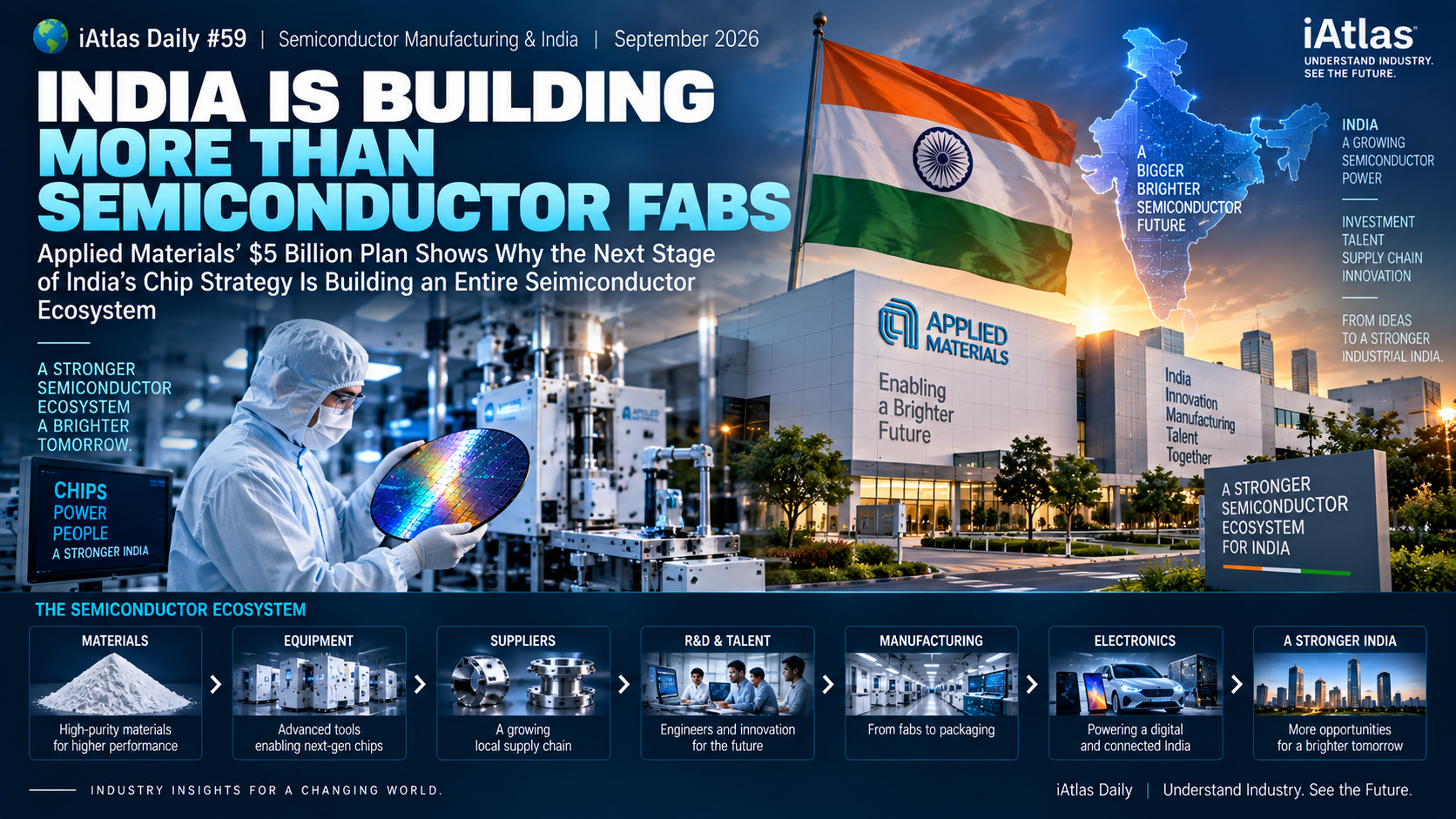
India Is Building More Than Semiconductor Fabs
Applied Materials’ $5 Billion Plan Shows Why the Next Stage of India’s Chip Strategy Is Building an Entire Semiconductor Ecosystem
📰 iAtlas Daily #59 | Semiconductor Manufacturing & India | September 2026
India wants to become a major semiconductor manufacturing hub.
But building semiconductor factories is only the beginning.
A modern semiconductor industry requires much more than fabs.
It requires:
Materials
↓
Equipment
↓
Suppliers
↓
Engineers
↓
R&D
↓
Manufacturing
↓
Packaging
↓
Customers
This is why the latest investment from Applied Materials matters.
At SEMICON India 2026, Applied Materials announced plans to invest more than $5 billion in India over the next decade, expanding its activities across research, supply-chain development and workforce capabilities.
The investment represents something larger than another semiconductor project.
It illustrates India’s transition from:
Attracting Semiconductor Factories
toward:
Building a Semiconductor Ecosystem
A country does not become a semiconductor hub simply by building a fab. It becomes one when the ecosystem around the fab begins to grow.
🌏 The Big Story
India has spent the past several years trying to establish itself as a new semiconductor manufacturing center.
The government has committed more than $21 billion to semiconductor incentives, while 12 semiconductor projects have been approved under its incentive programs. Commercial production has already begun at some packaging facilities.
Now another important layer is arriving.
Semiconductor Equipment
Applied Materials is one of the world’s largest semiconductor manufacturing-equipment companies.
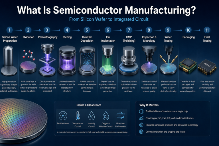
Its technologies are used across critical processes including:
Deposition
Materials Engineering
Etch
Ion Implantation
Process Control
and other manufacturing steps.
The company already describes India’s semiconductor and electronics manufacturing ecosystem as an important part of the future global semiconductor industry.
Its planned investment therefore sends an important signal.
Equipment companies are beginning to position themselves around India’s emerging semiconductor manufacturing base.
🏭 1. India’s First Goal Was Attracting Fabs
India historically played a significant role in semiconductor:
Design
Engineering
Software
But it had relatively little large-scale semiconductor manufacturing.
That began to change as the government introduced major semiconductor incentives.
The initial objective was straightforward:
Bring Chip Manufacturing to India
Projects began appearing across:
Wafer Fabrication
Assembly
Testing
Packaging
India’s ambition was to move from being primarily a semiconductor design and engineering location toward becoming a manufacturing location as well.
But that creates another challenge.
A semiconductor fab cannot operate alone.
🧩 2. A Semiconductor Fab Needs an Ecosystem
Imagine constructing a multibillion-dollar semiconductor factory.
The building is complete.
The cleanroom is ready.
But the factory still needs:
Manufacturing Equipment
Process Chemicals
Specialty Gases
Silicon Wafers
Quartz Components
Vacuum Systems
Precision Parts
Maintenance
Engineers
Logistics
Utilities
The real semiconductor industry therefore looks more like:
Materials
↓
Equipment
↓
Fab
↓
Packaging
↓
Electronics
A fab is only one layer.
This is precisely why equipment companies matter.
⚙️ 3. Applied Materials Sits Close to the Manufacturing Core
Applied Materials is not a chipmaker.
It builds technologies used to manufacture chips.
Its role becomes particularly important as semiconductor structures become more complex.
Modern semiconductor manufacturing increasingly requires atomic-level control over:
Materials
Film Thickness
Interfaces
Structures
Patterning
Applied describes its core position as materials engineering, with semiconductor scaling increasingly requiring new materials and more complex 3D structures.
This places companies like Applied at a critical point in the semiconductor value chain:
Chip Design
↓
Process Technology
↓
Manufacturing Equipment
↓
Wafer Fabrication
Without the equipment layer, fab capacity cannot become production capacity.
💰 4. Why the $5 Billion Number Matters
The headline number is significant:
More Than $5 Billion
over approximately ten years.
But the composition matters more than the number itself.
Reuters reports that Applied’s Indian investment is expected to support:
Research
Building deeper technical capabilities.
Supply-Chain Development
Expanding the network of suppliers supporting semiconductor manufacturing.
Workforce
Developing the engineers and technical talent needed for the industry.
That means the investment is not simply:
Build Factory → Produce Equipment
It is closer to:
R&D
Suppliers
Talent
Manufacturing Support
=
Ecosystem Development
🔬 5. R&D Changes the Nature of Localization
There is an important difference between manufacturing localization and technology localization.
The first stage is:
Make Products Locally
The deeper stage is:
Develop Technology Locally
R&D introduces:
Engineers
↓
Experiments
↓
Process Development
↓
Equipment Development
↓
Customer Collaboration
↓
Manufacturing
That creates capabilities that are harder to relocate.
A factory can theoretically move.
A dense network of engineering knowledge, suppliers and customers is much harder to reproduce elsewhere.
👨🔬 6. Talent May Be One of India’s Biggest Advantages
India already has a large engineering base.
Global semiconductor companies have operated design and engineering centers in the country for decades.
That provides India with an unusual starting point.
Many emerging semiconductor regions need to build both:
Engineering
and
Manufacturing
India already has significant capabilities on the engineering side.
The challenge is connecting that talent to:
Process Technology
Equipment
Fab Operations
Advanced Packaging
Manufacturing R&D
If that connection develops successfully, India’s existing engineering strength could become an important manufacturing advantage.
🔗 7. Suppliers Follow Manufacturing
This is one of the most important industrial patterns.
When a major factory is built, suppliers often begin moving closer.
Consider a semiconductor fab.
It needs continuous access to:
Chemicals
Gases
Components
Maintenance
Spare Parts
Technical Service
Long-distance supply chains can increase:
Lead Time
Inventory
Cost
Risk
As semiconductor manufacturing expands in India, the economic incentive for suppliers to establish local operations increases.
The sequence can become:
Fab
↓
Equipment Supplier
↓
Component Supplier
↓
Material Supplier
↓
Service Network
↓
Industrial Cluster
🇮🇳 8. India Is Beginning to Attract Multiple Layers
Applied Materials is not arriving in isolation.
Just one day after the Applied investment announcement, Dutch semiconductor company Nexperia announced a strategic partnership with Tata Electronics covering both wafer production and semiconductor packaging in India.
Nexperia plans to manufacture power-control chips at Tata’s Dholera facility and use Tata’s Jagiroad facility for assembly and testing.
That creates an interesting structure.
Tata
→ Semiconductor Manufacturing
Nexperia
→ Chip Technology / Products
Applied Materials
→ Equipment / Materials Engineering
Different companies occupy different layers.
That is exactly how ecosystems begin to form.
🏗️ 9. But India Still Has a Major Gap
India’s semiconductor ambitions are significant.
But the country is not yet a major wafer-fabrication center.
Reuters notes that although packaging plants have begun commercial production, India has not yet produced chips from a large-scale wafer fab.
Tata Electronics’ roughly $10 billion Gujarat fab has also experienced a delay of nearly two years.
This distinction is important.
Announcements are not the same as:
Installed Equipment
And installed equipment is not the same as:
Qualified Production
And qualified production is not the same as:
Competitive Yield
The semiconductor journey is long.
📈 10. India Has a Large Domestic Demand Advantage
India’s semiconductor strategy is supported by another important factor:
Demand
India expects semiconductor consumption to reach approximately $110 billion by 2030.
That demand can come from markets including:
Smartphones
Consumer Electronics
Automotive
Telecommunications
Industrial Equipment
Data Centers
Energy Systems
A large domestic market creates an important advantage.
Instead of building semiconductor manufacturing entirely for export, India can potentially connect local production to local electronics demand.
📱 11. Electronics Manufacturing Can Pull Semiconductors Behind It
This follows another familiar industrial pattern.
First:
Electronics Assembly
Then:
Components
Then:
Semiconductors
Then:
Equipment & Materials
The deeper the electronics manufacturing base becomes, the stronger the incentive to localize upstream components.
India has already become a major electronics manufacturing location.
Semiconductors represent the next strategic layer.
The long-term objective is therefore not merely:
Made in India Electronics
but increasingly:
Made in India Electronics
↓
using
Made in India Semiconductors
↓
supported by
India-Based Semiconductor Ecosystems
🌎 12. Geography Is Becoming More Important
India’s semiconductor push is happening during a broader restructuring of the global semiconductor map.
For decades, semiconductor manufacturing became highly concentrated across:
Taiwan
South Korea
China
Japan
United States
and parts of Southeast Asia.
Now governments and companies increasingly want:
Geographic Diversification
Supply-Chain Resilience
Alternative Manufacturing Hubs
India wants to become one of those hubs.
But the competition is intense.
The United States, Japan and Europe are also investing heavily in semiconductor manufacturing.
Japan and the U.S., for example, are reportedly discussing a new logic-chip fab that could cost roughly $13–19 billion, potentially operated by GlobalFoundries.
India is therefore competing for capital, equipment, suppliers and talent in a global semiconductor investment cycle.
🧱 13. Building the Fab Is Only Stage One
The development path can be divided into several stages.
Stage 1 — Investment
Government incentives and project announcements.
Stage 2 — Construction
Fab and packaging facilities.
Stage 3 — Equipment
Manufacturing tools are installed.
Stage 4 — Suppliers
Materials, components and services move closer.
Stage 5 — Talent
Engineers gain manufacturing experience.
Stage 6 — R&D
Technology begins to be developed locally.
Stage 7 — Ecosystem
The layers begin reinforcing each other.
India is currently trying to move through several of these stages simultaneously.
That is difficult.
But Applied’s investment is important because it directly addresses several of the middle layers.
🔄 14. Semiconductor Ecosystems Create Feedback Loops
Once a semiconductor ecosystem reaches sufficient scale, it can begin reinforcing itself.
More Fabs
↓
More Equipment Suppliers
↓
More Engineers
↓
More Local Suppliers
↓
Lower Operating Friction
↓
More Investment
↓
More Fabs
This is why established semiconductor clusters are so powerful.
Taiwan’s semiconductor strength is not simply TSMC.
South Korea’s is not simply Samsung Electronics and SK hynix.
Those companies sit inside broader networks of:
Materials
Equipment
Components
Universities
Engineers
Customers
Infrastructure
India ultimately needs the same type of network.
🧪 15. Materials Could Be the Next Layer
Once equipment and manufacturing expand, materials become increasingly important.
Semiconductor production consumes highly specialized materials including:
High-Purity Chemicals
Electronic Gases
Photoresists
Silicon Wafers
Quartz
Specialty Metals
This directly connects Daily #59 with Daily #54.
Daily #54 examined how semiconductor competition is moving upstream toward high-purity quartz.
Daily #59 shows the other side of the same process:
When a new semiconductor manufacturing hub emerges, upstream suppliers have a reason to follow.
This could eventually create new opportunities for material suppliers inside India.
📦 16. Packaging May Give India an Earlier Entry Point
India does not necessarily need to build every layer simultaneously.
Packaging and testing can provide an earlier path into semiconductor manufacturing.
Compared with the most advanced wafer fabs, assembly and packaging can have different capital and technology requirements.
India has already begun commercial production at some chip-packaging facilities.
This creates a possible progression:
Assembly & Test
↓
Advanced Packaging
↓
Manufacturing Experience
↓
Supplier Development
↓
Wafer Fabrication
The semiconductor ecosystem can therefore develop incrementally.
⚠️ 17. The Biggest Risk Is Execution
India’s semiconductor strategy has momentum.
But semiconductor manufacturing is unforgiving.
Success requires more than capital.
A fab must achieve:
Stable Production
High Yield
Reliable Utilities
Qualified Suppliers
Skilled Workforce
Customer Qualification
Continuous Technology Upgrades
This is why project delays matter.
India’s challenge over the next several years will be moving from:
Announcements
to
Production
and eventually:
Competitive Manufacturing
🏭 18. Applied Materials Is Also Expanding Globally
India should not be viewed in isolation from Applied’s broader strategy.
The company is simultaneously investing in major semiconductor ecosystems elsewhere.
Its new $5 billion EPIC Center in Silicon Valley is designed to bring chipmakers, equipment technology and R&D closer together and accelerate the transition from research to high-volume manufacturing.
Samsung Electronics, TSMC and SK hynix are among the companies participating in EPIC-related collaborations.
Applied has also expanded manufacturing in Singapore to support growing semiconductor-equipment demand.
This reveals a broader pattern.
Semiconductor equipment companies increasingly operate across a network of specialized regional ecosystems.
India is trying to become one of them.
🌐 19. The Semiconductor Map Is Becoming More Distributed
The old semiconductor map was highly concentrated.
The new map may become more distributed.
Not because existing hubs disappear.
They remain extraordinarily difficult to replace.
Instead, new hubs are emerging alongside them.
Potentially:
United States
→ Advanced Manufacturing & R&D
Taiwan
→ Leading-Edge Foundry
South Korea
→ Memory & Advanced Manufacturing
Japan
→ Materials & Equipment + New Fabs
Southeast Asia
→ Packaging & Manufacturing
India
→ Design + Packaging + Emerging Fab Ecosystem
The important question is not whether India replaces another semiconductor hub.
It is:
Which layers of the global semiconductor stack can India successfully capture?
🧩 Why This Matters
Applied Materials’ investment highlights several important changes.
India’s semiconductor strategy is entering a second phase.
The focus is expanding beyond individual fab announcements.
Equipment companies matter.
Manufacturing cannot scale without the equipment and process ecosystem behind it.
R&D is strategically important.
Local technology development creates deeper capabilities than manufacturing alone.
Suppliers can follow fabs.
New manufacturing capacity creates incentives for materials, components and service companies to localize.
Execution remains the key test.
India still needs to convert investment announcements into competitive high-volume production.
🔭 What to Watch
Applied Materials’ $5B Investment
Watch where capital is allocated across R&D, supply-chain development and workforce expansion.
Tata Electronics
The progress of Tata’s Dholera fab will be one of the most important indicators of India’s wafer-manufacturing ambitions.
Nexperia–Tata
The new partnership provides another test of whether India can connect global chip technology with domestic manufacturing.
Semiconductor Materials
Watch whether chemical, gas, wafer and precision-component suppliers begin establishing larger Indian operations.
Advanced Packaging
Packaging may become one of India’s strongest early semiconductor manufacturing positions.
Talent
The ability to convert India’s engineering base into manufacturing expertise will be critical.
Yield
Ultimately, the most important semiconductor metric is not announced investment.
It is whether fabs can produce chips reliably and economically.
🧭 iAtlas Insight
India’s semiconductor strategy is reaching an important transition.
The first question was:
Can India attract semiconductor factories?
The next question is harder:
Can India build the ecosystem those factories require?
Applied Materials’ planned investment matters because it sits precisely at that transition.
The semiconductor stack looks like:
Talent & R&D
↓
Materials
↓
Equipment
↓
Fab
↓
Packaging
↓
Electronics
↓
Market
India already has strengths at both ends:
Engineering talent
and
A huge electronics market.
What it is trying to build is everything in between.
If those layers begin connecting, India’s semiconductor ambitions could become much more durable.
Because ultimately:
A fab creates production capacity. An ecosystem creates an industry.
📚 Related Articles
📰 iAtlas Weekly #11: Industrial Competition Is Moving Deeper into the Supply Chain
📰 Daily #54 — Semiconductor Materials: High-Purity Quartz / Semiconductor Materials
🔗 References
Reuters — Applied Materials to Invest $5 Billion in India
Applied Materials — SEMICON India 2026
Applied Materials — EPIC Center & TSMC Partnership
ℹ️ About iAtlas
iAtlas is an independent publication covering batteries, semiconductors, OLED, advanced materials, AI, and global industrial trends.
We transform complex industrial developments into clear, reliable, and easy-to-understand insights.
Whether you’re following today’s industry news or building long-term expertise, iAtlas helps you understand not only what happened, but why it matters.
Technology creates change.
Insight creates opportunity.
— iAtlas