SK hynix Expands AI Memory Beyond HBM
From HBM to Enterprise SSDs, AI Infrastructure Is Becoming a Full Memory Opportunity
📊 iAtlas Daily #42 | Semiconductor & AI Infrastructure | August 2026
🌍 The Big Story
The SK hynix AI Memory strategy is expanding beyond HBM as the company builds a broader portfolio spanning DRAM, enterprise SSDs and computational storage for AI infrastructure.
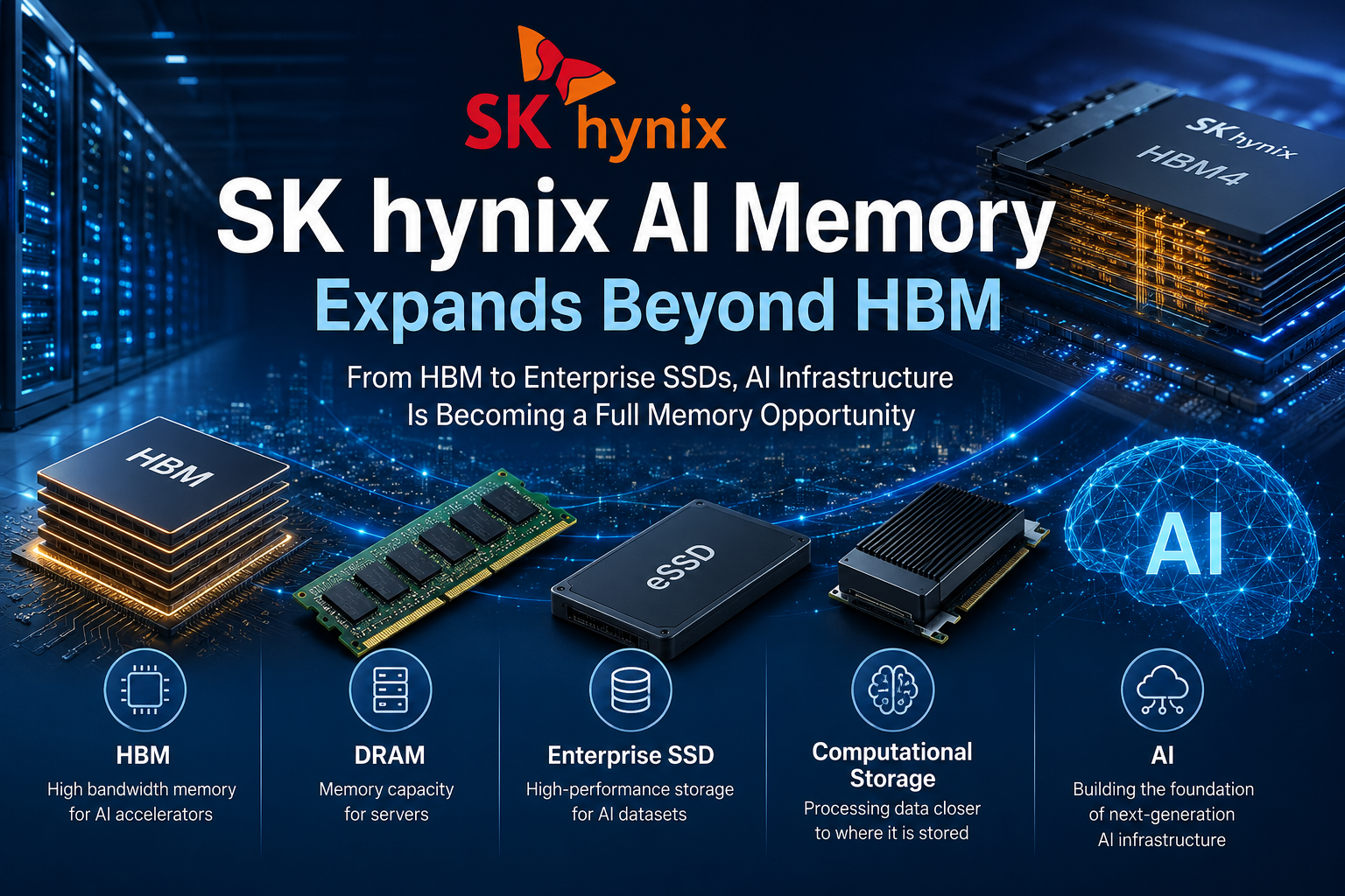
On August 26, SK hynix presented a broad portfolio of memory solutions designed for AI infrastructure, covering HBM, DRAM, enterprise SSDs (eSSD), and computational storage SSDs (cSSD).
The development highlights an important shift in the semiconductor industry.
AI infrastructure is no longer simply about supplying the fastest memory next to GPUs.
As AI systems grow larger, data must move through multiple layers of infrastructure—from storage and servers to accelerators and networking.
That is turning the entire memory hierarchy into part of the AI infrastructure race.
🧠 Why AI Needs More Than HBM
HBM has become one of the most important semiconductor technologies of the AI era.
Placed close to GPUs and AI accelerators, HBM provides the enormous memory bandwidth required to process large AI workloads.
But HBM alone cannot support an entire AI data center.
AI infrastructure also requires:
HBM
↓
High-speed memory for AI accelerators
Server DRAM
↓
Memory capacity for CPUs and servers
Enterprise SSDs
↓
Large-scale storage for AI datasets
Computational Storage
↓
Processing data closer to where it is stored
The result is a much larger opportunity.
Instead of competing for a single component, memory manufacturers increasingly have an opportunity to supply multiple layers of the AI computing architecture.
💾 NAND Is Becoming Part of the AI Story
This trend is particularly important for NAND flash.
AI models require enormous datasets.
Those datasets must be stored, accessed and continuously transferred between storage systems and computing infrastructure.
As AI workloads grow, enterprise SSD performance increasingly matters for:
- AI training datasets
- inference workloads
- vector databases
- cloud AI services
- data-center storage
- retrieval-augmented generation
This means AI growth could increasingly influence not only HBM demand but also the enterprise NAND and SSD markets.
For SK hynix, this creates an opportunity to connect its DRAM and HBM leadership with the NAND and enterprise SSD capabilities of its broader storage business.
⚡ The Next Bottleneck: Moving Data
The semiconductor industry has spent years improving computing performance.
But increasingly, the challenge is not simply:
How fast can we calculate?
It is:
How efficiently can we move data?
Moving huge amounts of information between storage, memory and processors consumes energy and creates latency.
This is why technologies such as computational storage are gaining attention.
Rather than repeatedly transferring all data back to the CPU or accelerator, some processing can occur closer to the storage device itself.
For large AI infrastructure, reducing unnecessary data movement could become increasingly valuable.
🧩 HBM Technology Is Also Changing
At the same time, HBM itself continues to evolve.
SK hynix recently highlighted hybrid bonding as an important technology for future semiconductor packaging. Its August 25 technology note describes hybrid bonding as a foundational technology for improving semiconductor performance, with relevance to advanced HBM generations.
The issue is physical.
As HBM adds more stacked memory layers, manufacturers must maintain strict package-height limits while increasing capacity and performance.
Traditional bonding technologies therefore face increasingly difficult scaling challenges.
Hybrid bonding can connect dies with much finer interconnect structures, potentially enabling:
More memory layers -> Higher bandwidth -> Greater capacity ->
Thinner interconnects -> Improved power efficiency
Industry reporting around Hot Chips 2026 indicates that SK hynix expects hybrid bonding to become particularly important further along the HBM roadmap, while existing packaging technologies continue to support nearer-term generations.
🏭 Why This Matters for the Semiconductor Supply Chain
The expansion of AI memory creates opportunities well beyond memory manufacturers.
Advanced Packaging
More complex HBM architectures require increasingly sophisticated stacking, bonding and inspection processes.
Semiconductor Equipment
Hybrid bonding and advanced packaging increase requirements for wafer preparation, bonding, metrology and inspection equipment.
Materials
Advanced packaging requires increasingly precise dielectric materials, bonding interfaces and process chemicals.
NAND & SSD
AI data centers create another structural demand driver for high-performance enterprise storage.
Thermal Management
Higher-density computing and memory architectures increase the importance of cooling and power management.
The AI memory boom is therefore becoming a broader semiconductor manufacturing ecosystem opportunity.
📊 The Bigger Picture
The first phase of the AI semiconductor boom was dominated by GPUs.
The second phase brought HBM into the spotlight.
The next phase may be broader.
AI Accelerators -> HBM -> Server DRAM -> Enterprise SSD -> AI Storage ->
Networking -> Advanced Packaging
Each layer must improve for AI infrastructure to continue scaling.
That means the AI semiconductor opportunity is gradually moving from individual chips toward complete computing systems.
The SK hynix AI Memory portfolio shows how the AI semiconductor opportunity is expanding from individual chips toward complete computing systems.
🔎 What to Watch
The next developments worth watching are:
HBM4 and future HBM architectures — how quickly bandwidth and capacity continue increasing.
Hybrid bonding — when it becomes economically viable for high-volume HBM manufacturing.
Enterprise SSD demand — whether AI data centers become a major structural growth driver for NAND.
Computational storage — whether processing closer to storage becomes widely adopted in AI infrastructure.
AI memory competition — how Samsung Electronics, SK hynix and Micron differentiate increasingly broad AI-memory portfolios.
💡 iAtlas Insight
AI infrastructure is becoming a data-movement problem as much as a computing problem.
GPUs provide computing power.
HBM feeds the accelerator.
DRAM supports servers.
Enterprise SSDs store enormous datasets.
Advanced packaging connects increasingly complex semiconductor architectures.
The companies that can optimize several of these layers together may capture a larger share of AI infrastructure investment.
SK hynix’s expanding AI-memory portfolio illustrates this transition clearly:
The AI memory race is evolving from HBM competition into a full memory-system competition.
🔗 Related Articles
iAtlas Daily #41: YMTC Targets $4.9 Billion IPO to Expand China’s Memory Chip Industry
iAtlas Daily #11: SK hynix US IPO Raises $26.5 Billion for AI Memory Expansion
iAtlas Daily #10: TSMC Advanced Packaging Expansion Signals the Next AI Boom
🔗 Sources
- SK hynix Newsroom — SK hynix Presents a Full Lineup of Memory Solutions Optimized for AI Infrastructure at DTF 2026
- SK hynix Newsroom — Hybrid Bonding: Evolving into a Foundational Technology for Improving Semiconductor Performance
- Tom’s Hardware — SK hynix Pushes Hybrid Bonding to HBM5 as AI Memory Hits 775-Micron Ceiling
About iAtlas
iAtlas is an independent publication covering batteries, semiconductors, OLED, advanced materials, AI, and global industrial trends.
We transform complex industrial developments into clear, reliable, and easy-to-understand insights.
Whether you’re following today’s industry news or building long-term expertise, iAtlas helps you understand not only what happened, but why it matters.
Technology creates change.
Insight creates opportunity.
— iAtlas