Applied Materials Expands for the AI Chip Boom
Why AI Demand Is Moving Deeper Into Semiconductor Equipment
📰 iAtlas Daily #36 | August 2026
📰 What Happened?
The AI investment boom is moving deeper into the semiconductor supply chain.
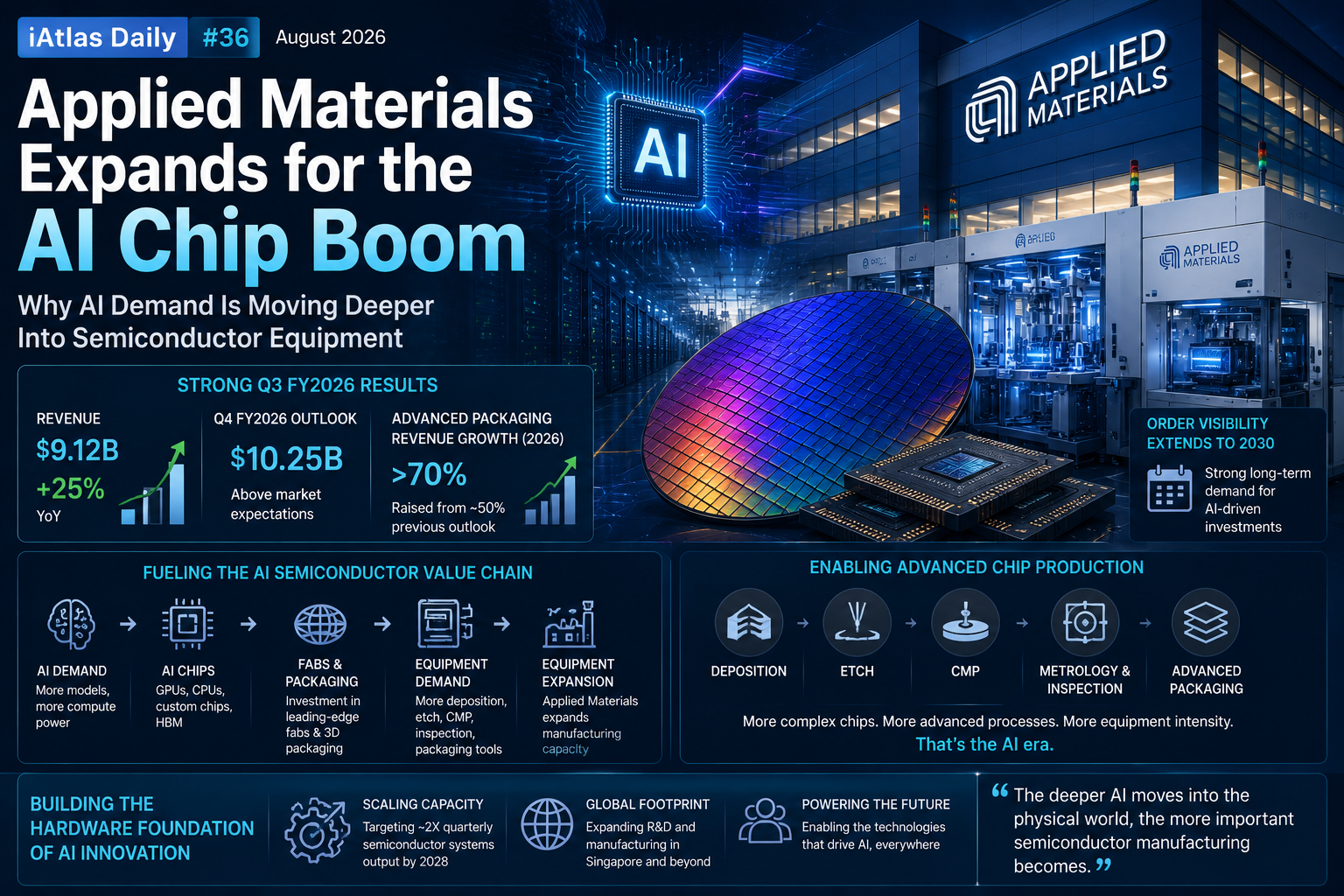
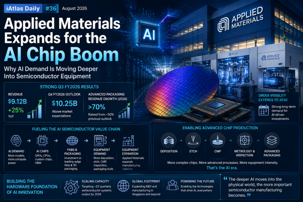
Applied Materials, one of the world’s largest semiconductor equipment companies, reported fiscal third-quarter 2026 revenue of approximately $9.12 billion, up about 25% year over year, as demand for advanced semiconductor manufacturing equipment remained strong.
The company also expects fiscal fourth-quarter revenue of around $10.25 billion, above market expectations.
But the bigger story is not simply another strong earnings report.
Applied Materials is preparing for a much larger manufacturing cycle driven by AI.
The company plans to expand its ability to supply semiconductor manufacturing systems as customers invest in:
- Advanced logic
- DRAM
- High Bandwidth Memory
- Advanced packaging
- AI computing infrastructure
The message is becoming increasingly clear:
The AI boom is no longer just a GPU story. It is becoming a semiconductor equipment story.
💡 Why This Matters
AI Chips Require More Than More Fabs
When AI semiconductor demand is discussed, attention usually goes to companies such as NVIDIA, TSMC, SK hynix, and other chip manufacturers.
But chips cannot be produced without semiconductor equipment.
Every advanced semiconductor requires dozens—or even hundreds—of manufacturing steps involving:
Deposition → Etching → Patterning → Cleaning → CMP → Inspection → Packaging
As semiconductor structures become more complex, the number and difficulty of these processes can increase.
That creates an important consequence.
Even if wafer volumes do not increase at the same rate as AI computing demand, equipment intensity per advanced chip can continue rising.
🧠 HBM Is Creating New Equipment Demand
One of the strongest examples is HBM.
AI accelerators require enormous memory bandwidth, pushing semiconductor manufacturers toward increasingly complex HBM architectures.
But producing HBM is much more difficult than simply manufacturing conventional DRAM.
Multiple memory dies must be manufactured, processed, stacked, interconnected, inspected, and packaged with extremely high precision.
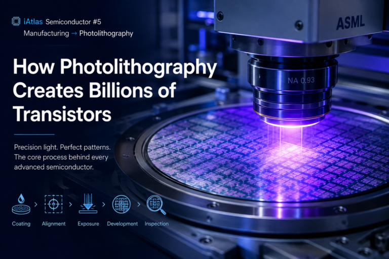
Applied Materials introduced new systems in June specifically targeting next-generation DRAM and advanced packaging for AI chips, including equipment for epitaxy, CMP, deposition and eBeam metrology.
The company says AI computing is increasingly encountering a memory wall, making HBM and 3D integration critical to improving system performance.
That creates new opportunities for semiconductor equipment companies.
📦 Advanced Packaging Is Becoming a Growth Engine
Perhaps the most interesting number from Applied Materials’ latest outlook concerns advanced packaging.
The company now expects its advanced packaging revenue to grow more than 70% in calendar 2026, up from its previous expectation of around 50%.
Why?
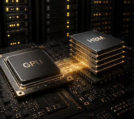
Modern AI processors are increasingly assembled as complex systems rather than single chips.
A high-performance AI package may integrate:
GPU / Accelerator + Multiple HBM Stacks + I/O Chips + Interposer / Substrate
All of these components must operate together at extremely high speeds.
That makes packaging increasingly important to overall system performance.
In other words:
Packaging is becoming part of semiconductor performance engineering.
⚙️ Applied Materials Is Increasing Manufacturing Capacity
Applied Materials is also preparing its own manufacturing infrastructure for this demand.
In June, the company opened a new $500 million manufacturing and R&D campus in Singapore.
The Tampines facility more than doubles Applied Materials’ advanced cleanroom capacity in Singapore and is already operating at volume production.
More recently, the company indicated that it is preparing to substantially increase semiconductor system production capacity.
According to the Wall Street Journal, Applied Materials is targeting roughly double its quarterly semiconductor systems output by 2028, while preparing for potentially greater demand through 2030.
That is significant.
Equipment manufacturers themselves are now having to scale for the AI investment cycle.
🏭 From Fab Expansion to Equipment Expansion
This creates an interesting chain reaction.
Stage 1 — AI Demand
More AI models and services require more computing power.
↓
Stage 2 — Semiconductor Demand
More computing requires GPUs, CPUs, networking chips, and HBM.
↓
Stage 3 — Fab & Packaging Investment
Chipmakers expand manufacturing and advanced packaging capacity.
↓
Stage 4 — Equipment Demand
Those factories require more deposition, etch, CMP, metrology, inspection, and packaging equipment.
↓
Stage 5 — Equipment Manufacturing Expansion
Equipment companies must expand their own production capacity.
The AI manufacturing cycle is therefore moving increasingly far upstream.
🔬 More Complex Chips Mean More Complex Equipment
Another important trend is semiconductor architecture.
Traditional semiconductor scaling relied heavily on shrinking features horizontally.
But the industry is increasingly moving into the third dimension.
Examples include:
- Gate-All-Around transistors
- 3D NAND
- HBM stacking
- Chiplets
- Hybrid bonding
- Advanced packaging
Applied Materials has recently introduced new deposition and selective etch systems designed specifically for increasingly deep and narrow 3D semiconductor structures.
As chip structures become more three-dimensional, controlling materials at atomic-scale precision becomes increasingly difficult.
That makes process equipment more strategically important.
🌍 Industry Impact
⚙️ Semiconductor Equipment
AI could support a multi-year investment cycle across deposition, etching, CMP, inspection, metrology, and packaging equipment.
🧠 Memory
HBM and next-generation DRAM require increasingly sophisticated manufacturing processes.
📦 Advanced Packaging
Packaging equipment could become one of the semiconductor industry’s fastest-growing equipment categories.
🧪 Semiconductor Materials
More complex processes increase demand for specialty gases, chemicals, deposition precursors, CMP materials, and other advanced materials.
🏭 Semiconductor Fabs
Equipment availability and installation capacity could become increasingly important as manufacturers simultaneously expand AI-related production.
👀 What to Watch
Several indicators will show how far the current equipment cycle can run:
- HBM capacity expansion
- Advanced packaging investment
- TSMC and memory-maker capital spending
- Applied Materials manufacturing expansion
- Semiconductor equipment order backlog
- DRAM investment
- 2nm and next-generation logic ramps
- AI data-center spending
But one development deserves particular attention:
Advanced packaging equipment growth.
If Applied Materials’ projected 70%+ growth materializes, it would provide another strong indication that packaging is becoming one of the semiconductor industry’s major investment frontiers.
🎯 Atlas Insight
The AI semiconductor boom is moving upstream.
At first, investors focused on NVIDIA.
Then attention moved toward HBM manufacturers.
Then advanced packaging became a bottleneck.
Now semiconductor equipment is entering the spotlight.
The industrial chain increasingly looks like this:
AI Infrastructure
↓
AI Chips
↓
HBM & Advanced Packaging
↓
Semiconductor Fabs
↓
Equipment
↓
Materials & Components
Each layer creates demand for the layer beneath it.
That is why Applied Materials’ latest results matter.
They show that AI investment is no longer concentrated only among the companies designing and manufacturing chips.
It is spreading into the industrial infrastructure required to manufacture those chips at scale.
And as semiconductor architectures become more complex, equipment may become an even more important part of the AI technology race.
The deeper AI moves into the physical world, the more important semiconductor manufacturing becomes.
📚 Related Articles
📰 iAtlas Daily #23 | TSMC Expands Advanced Packaging Capacity
📰 iAtlas Daily #30 | SK hynix Invests ₩54 Trillion in New Memory Fabs
📊 iAtlas Weekly #6 | Scale Is Becoming the New Industrial Advantage
Sources
- Applied Materials — 3D Deposition & Etch Systems
- Applied Materials — New Systems for DRAM and Advanced Packaging
- Applied Materials — Singapore Manufacturing Expansion
- Reuters — Applied Materials Q3 2026 Results and Outlook
- The Wall Street Journal — Applied Materials Capacity Expansion
About iAtlas
iAtlas is an independent publication covering batteries, semiconductors, OLED, advanced materials, AI, and global industrial trends.
We transform complex industrial developments into clear, reliable, and easy-to-understand insights.
Whether you’re following today’s industry news or building long-term expertise, iAtlas helps you understand not only what happened, but why it matters.
Technology creates change.
Insight creates opportunity.
— iAtlas