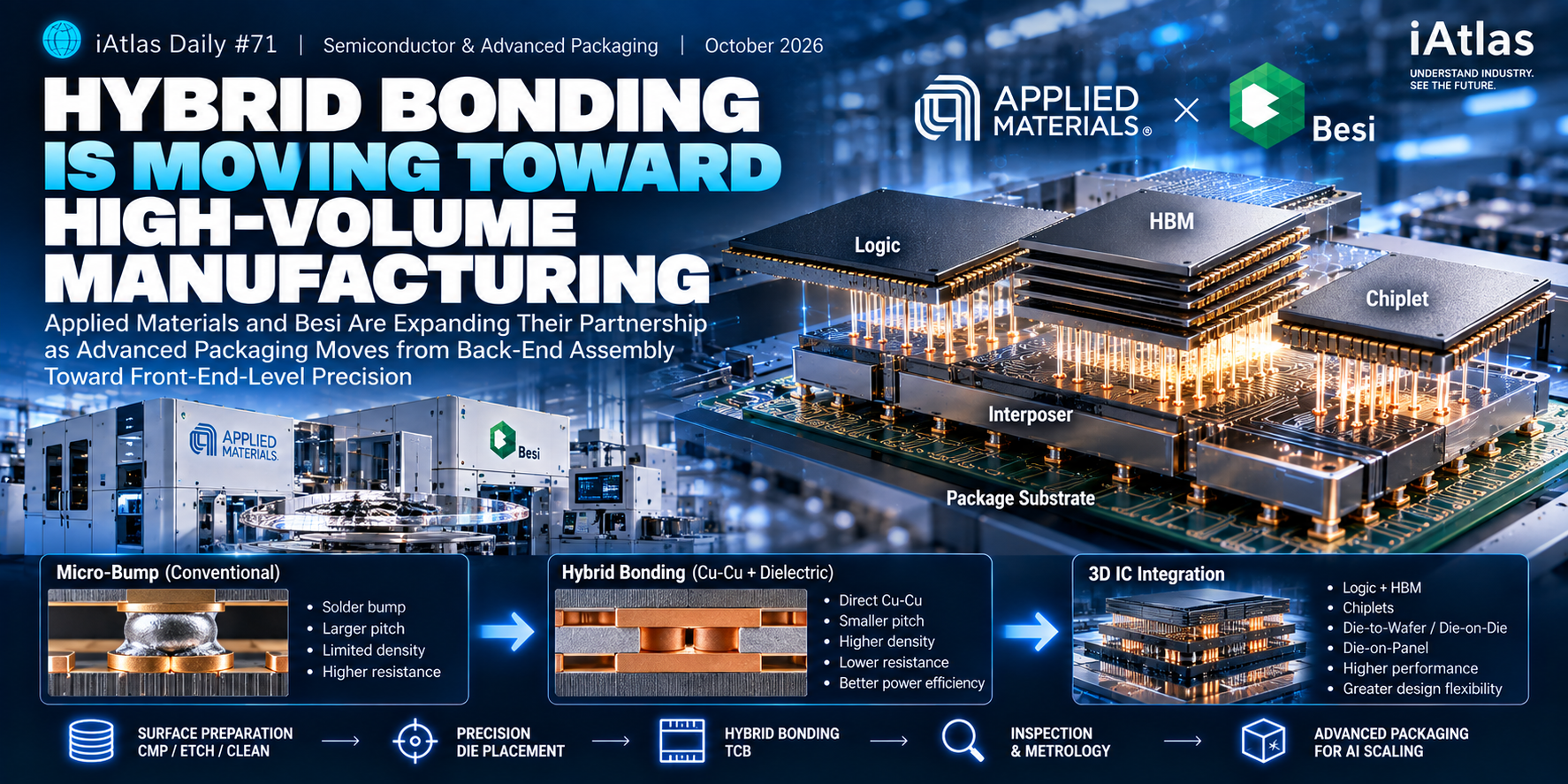
Hybrid Bonding Is Moving Toward High-Volume Manufacturing
Applied Materials and Besi Are Expanding Their Partnership as Advanced Packaging Moves from Back-End Assembly Toward Front-End-Level Precision
🔲 iAtlas Daily #71 | Semiconductor & Advanced Packaging | October 2026

For decades, semiconductor performance improved through a relatively straightforward strategy:
Make Transistors Smaller
Smaller transistors enabled more computing power to fit inside a chip.
But modern semiconductor systems are becoming more complicated.
AI accelerators increasingly combine:
Logic
HBM
Chiplets
Advanced Packaging
and:
High-Speed Interconnects
Instead of relying entirely on one large monolithic chip.
This creates a new problem.
The individual dies may be extremely advanced.
But they still need to communicate with each other.
And as the number of connections increases, the technology used to connect those dies becomes increasingly important.
That is where:
Hybrid Bonding
enters the picture.
On October 1, Applied Materials and Besi announced an expansion of their strategic partnership covering hybrid bonding, thermo-compression bonding and new die integration architectures.
The collaboration is moving beyond:
Die-to-Wafer
toward:
Die-on-Wafer
Die-on-Die
Die-on-Panel
and other advanced integration platforms. Applied Materials
The announcement points toward a larger change in semiconductor manufacturing.
Advanced packaging is becoming less like conventional assembly and more like precision semiconductor manufacturing.
🌍 The Big Story
Traditional semiconductor manufacturing was often divided into two broad worlds.
Front-End
Where transistors and circuits are fabricated on wafers.
This requires:
Extreme Precision
Clean Environments
Deposition
Etching
Planarization
Metrology
and:
Defect Control
Then came:
Back-End
Where chips were:
Cut
Connected
Packaged
and:
Assembled
Historically, much of the industry’s technological attention focused on the front end.
But advanced packaging is changing that distinction.
The connections between chips are becoming so small and so dense that packaging increasingly requires:
Front-End-Level Precision
Applied Materials now explicitly describes advanced packaging as a materials-engineering challenge requiring precision and cleanliness comparable to front-end wafer fabrication. Applied Materials
1. Why Do Chips Need to Be Bonded?
A modern semiconductor system may contain multiple specialized dies.
For example:
Compute Die
I/O Die
HBM
Other Chiplets
These components need to exchange enormous amounts of data.
Traditionally, electrical connections between semiconductor components could be created using structures such as:
Solder Bumps
or:
Micro-Bumps
These technologies remain extremely important.
But as interconnect density increases, the physical size and spacing of those connections become increasingly challenging.
The industry therefore needs another way to connect chips at much finer pitches.
2. What Is Hybrid Bonding?
Hybrid bonding combines two connections at the same interface.
Metal-to-Metal
and:
Dielectric-to-Dielectric
The most important electrical connection is typically:
Copper → Copper
Instead of relying on a solder bump between the two dies, copper surfaces can be directly connected.
This can create:
Smaller Interconnect Pitch
Higher Connection Density
Shorter Electrical Paths
and:
Improved Power Efficiency
Applied Materials describes direct copper-to-copper bonding as a way to increase interconnect density while shortening wiring between chiplets. Applied Materials
3. Why Does Interconnect Pitch Matter?
Imagine two chips that need to communicate.
If the connections are relatively large, only a limited number can fit within a given area.
Reduce their size and spacing, and many more connections can fit.
Conceptually:
Large Pitch
● ● ● ●
versus:
Fine Pitch
● ● ● ● ● ● ● ● ● ●
More connections allow more data to move between dies simultaneously.
That becomes particularly important for:
High-Bandwidth Computing
4. HBM Makes the Problem Easy to See
High Bandwidth Memory demonstrates why packaging interconnects matter.
HBM increases bandwidth partly by placing memory physically close to the processor and using a very wide interface.
The system therefore depends on more than:
Fast DRAM
It also depends on:
TSVs
Interposers
Advanced Packaging
and:
Dense Interconnects
As compute and memory become more tightly integrated, the connection between them becomes part of overall system performance.
The package is no longer simply protecting the chip.
The package is becoming part of the computing architecture.
5. Micro-Bumps Cannot Shrink Forever
Micro-bump technology has enabled advanced packaging for years.
But shrinking bumps creates challenges.
These can include:
Pitch Scaling
Solder Volume
Alignment
Electrical Resistance
and:
Thermal Behavior
At sufficiently fine dimensions, continuing to scale conventional solder-based connections becomes increasingly difficult.
Hybrid bonding provides another path.
Instead of:
Chip
↓
Solder Bump
↓
Chip
the connection can move toward:
Copper
↓
Direct Copper Bond
↓
Copper
This removes the solder layer from the connection.
6. But Direct Bonding Is Much Harder Than It Sounds
Two copper surfaces cannot simply be pushed together casually.
The surfaces must be prepared with extraordinary precision.
Successful hybrid bonding depends on factors such as:
Surface Flatness
Surface Cleanliness
Alignment Accuracy
Particle Control
Copper Surface Quality
and:
Bonding Conditions
A tiny particle can prevent proper bonding.
A small height variation can create defects.
A small alignment error can compromise electrical connections.
That is why hybrid bonding begins to resemble front-end semiconductor processing.
7. CMP Becomes Critical
One important process is:
Chemical Mechanical Planarization — CMP
Before bonding, the surface needs to be extremely flat.
If one region is slightly higher than another, uniform bonding becomes difficult.
CMP combines:
Chemical Reactions
and:
Mechanical Polishing
to create highly planar surfaces.
This is already a fundamental process in semiconductor wafer fabrication.
Hybrid bonding brings this type of front-end process discipline deeper into packaging.
8. Cleaning Becomes Critical Too
Particles that appear insignificant at normal scale can become enormous relative to a fine-pitch bonding interface.
This means hybrid bonding requires extremely strong:
Contamination Control
Applied Materials and Besi’s joint development combines capabilities spanning:
Etch
Planarization
Deposition
Wafer Cleaning
Metrology
Inspection
and:
Particle Defect Control
with Besi’s:
Die Placement
Interconnect
and:
Assembly
technology. Applied Materials
That combination tells us something important.
Hybrid bonding is not one machine.
It is:
A Process Flow
9. Alignment Becomes Another Major Challenge
Imagine bonding millions of microscopic electrical connections.
Every connection needs to align with its counterpart.
As pitch becomes smaller:
Alignment Error Tolerance
↓
decreases.
That makes precision die placement increasingly important.
This is where Besi’s expertise becomes particularly relevant.
Its assembly technology focuses on placing and connecting dies with the accuracy and throughput needed for advanced packaging.
10. Applied Materials and Besi Bring Different Strengths
The partnership combines two different areas of semiconductor manufacturing.
Applied Materials
Brings expertise in:
Materials Engineering
Surface Preparation
CMP
Deposition
Etch
Cleaning
Inspection
and:
Metrology
Besi
Brings expertise in:
Die Placement
Bonding
Interconnect
and:
Assembly
Together:
Surface Preparation
↓
Precision Placement
↓
Bonding
↓
Inspection
become a more integrated manufacturing flow.
11. Their Collaboration Started Years Ago
The partnership itself is not new.
Applied Materials and Besi began collaborating in:
2020
The companies established a:
Hybrid Bonding Center of Excellence
at Applied Materials’ Advanced Packaging Development Center in Singapore. Applied Materials
That collaboration eventually produced:
Kinex™
which Applied describes as the industry’s first integrated die-to-wafer hybrid bonding system. Applied Materials
The October 2026 announcement expands that relationship further.
12. Applied Materials Also Invested in Besi
The relationship became even deeper in 2025.
Applied Materials purchased approximately:
9%
of Besi’s outstanding shares.
Applied described the investment as a long-term strategic commitment to hybrid bonding and advanced packaging. Applied Materials
This is important because equipment companies are not merely selling independent machines.
They are increasingly collaborating to develop:
Integrated Manufacturing Solutions
13. The Partnership Is Now Expanding Again
The October 2026 announcement broadens the collaboration.
Besi is joining Applied Materials’:
EPIC Center
as an Innovation Partner.
The companies plan to work across:
Next-Generation Hybrid Bonding
Thermo-Compression Bonding
3D IC Integration
Logic + Memory Integration
and:
Photonics
The objective is to shorten the path from:
Technology Development
to:
High-Volume Manufacturing Applied Materials
14. The Architecture Is Expanding Too
The original collaboration centered heavily on:
Die-to-Wafer Hybrid Bonding
But future packaging architectures are becoming more diverse.
Applied and Besi specifically identify:
Die-on-Wafer
Die-on-Die
and:
Die-on-Panel
integration platforms among planned R&D areas. Applied Materials
Why does this matter?
Because advanced packaging is no longer converging around one universal architecture.
Different semiconductor systems may require different integration methods.
15. Die-to-Wafer
In die-to-wafer integration:
Individual Dies
↓
are placed onto:
A Wafer
This can be useful when known-good dies need to be selectively integrated.
Instead of bonding an entire wafer to another wafer, manufacturers can choose individual dies.
That provides more flexibility for heterogeneous integration.
16. Die-on-Die
Another architecture directly stacks:
Die
↓
Die
This can create highly compact 3D structures.
Potential applications include increasingly tight integration between:
Logic
Memory
and:
Specialized Accelerators
The shorter the physical distance between computing elements, the greater the opportunity to reduce interconnect energy and increase bandwidth.
17. Die-on-Panel Could Change Scale
Perhaps one of the most interesting directions is:
Die-on-Panel
Instead of integrating devices only at wafer scale, manufacturers explore much larger panel formats.
Larger processing areas could potentially improve manufacturing economics.
But they also create major challenges involving:
Warpage
Uniformity
Alignment
Handling
and:
Yield
This connects directly with another emerging advanced-packaging technology:
Glass Substrates
18. Glass Substrates and Hybrid Bonding Are Part of the Same Story
In Daily #69, we examined why glass substrates are attracting attention.
As semiconductor packages become larger, the industry needs:
Greater Dimensional Stability
Lower Warpage
Fine Wiring
and:
Larger Package Formats
Hybrid bonding addresses another part of the same problem.
Glass substrate asks:
What platform should increasingly complex packages be built on?
Hybrid bonding asks:
How should increasingly complex dies be connected?
Together they illustrate the changing architecture of advanced packaging.
19. Advanced Packaging Is Becoming a System
The industry once talked about packaging as though it were a final manufacturing step.
Now advanced packaging involves:
Substrate
Interposer
Chiplets
HBM
Bonding
Thermal Management
Inspection
The interaction among these technologies determines system performance.
That makes packaging increasingly:
A Systems Engineering Problem
20. Thermo-Compression Bonding Is Not Disappearing
Hybrid bonding receives enormous attention.
But this does not mean every semiconductor package will immediately switch to hybrid bonding.
Applied Materials and Besi are also expanding work on:
Thermo-Compression Bonding — TCB
TCB uses heat and pressure to form connections between dies and substrates.
It remains important in advanced packaging and memory integration.
The expanded partnership explicitly includes scaling TCB and its surrounding process ecosystem. Applied Materials
This again suggests that future packaging will use:
Multiple Bonding Technologies
depending on application.
21. Hybrid Bonding Must Solve the Manufacturing Equation
A technology can demonstrate excellent performance in a laboratory.
But high-volume manufacturing asks different questions.
Can it achieve:
High Throughput?
High Yield?
Low Defect Density?
Repeatability?
Acceptable Cost?
Hybrid bonding needs to satisfy all of them.
That is why the transition from:
Technology Demonstration
to:
High-Volume Manufacturing
is so important.
22. Yield Can Decide Everything
Suppose a complex package contains multiple expensive dies.
If one bonding defect causes the entire package to fail, the economic loss can be significant.
As package value rises:
Yield Becomes More Valuable
This increases demand for:
Inspection
Metrology
Known-Good-Die Strategies
and:
Process Control
Advanced packaging therefore creates opportunities far beyond bonding equipment itself.
23. Inspection Moves Earlier into the Process
Traditional quality control can sometimes detect problems after assembly.
That becomes increasingly expensive for advanced packages.
Instead, manufacturers want to detect defects:
Before Value Is Added
That means inspection may occur repeatedly throughout:
Surface Preparation
↓
Die Placement
↓
Bonding
↓
Final Integration
The higher the package value, the more important early defect detection becomes.
24. Equipment Integration Could Become a Competitive Advantage
Historically, semiconductor manufacturing lines contain equipment from many specialized vendors.
Each tool performs a particular process.
But as process windows become narrower, optimizing each machine independently may not be enough.
Hybrid bonding requires interactions between:
CMP
Cleaning
Metrology
Placement
and:
Bonding
That creates demand for:
Co-Optimized Process Flows
This is exactly the direction Applied Materials and Besi emphasize in their expanded collaboration. Applied Materials
25. The EPIC Center Is Designed Around That Idea
Applied Materials is building its new:
EPIC Center
in Silicon Valley.
The company says capital spending is expected to scale over time to approximately:
$5 Billion
as customer projects commence. Applied Materials
The center is intended to bring:
Chipmakers
Equipment Companies
Materials Suppliers
and:
Technology Partners
closer together during development.
The objective is to reduce the time required to move technologies from:
Research
to:
Commercial Manufacturing
26. Packaging Innovation Is Becoming Collaborative
This is another important industry change.
Advanced packaging increasingly requires expertise from multiple companies.
One company may specialize in:
Wafer Processing
another in:
Bonding
another in:
Substrates
another in:
Inspection
another in:
Materials
The technology becomes too interconnected for every company to optimize its component independently.
Innovation therefore increasingly happens through:
Ecosystems
27. AI Is the Demand Driver, Not the Whole Story
AI is clearly accelerating advanced-packaging investment.
But hybrid bonding should not be understood only as:
An AI Technology
The underlying trend is broader.
Semiconductor systems increasingly use:
Heterogeneous Integration
because integrating different specialized dies can provide advantages in:
Performance
Power
Cost
and:
Design Flexibility
AI makes the need more urgent.
But the manufacturing capability can ultimately support a wider range of semiconductor systems.
28. Logic and Memory Are Moving Closer Together
One particularly important direction is:
Logic + Memory Integration
Moving memory closer to compute reduces the physical distance data needs to travel.
That can improve:
Bandwidth
and:
Energy Efficiency
This is critical because moving data itself consumes significant energy.
Future performance gains may therefore come not only from faster transistors.
They may come from:
Better Connections Between Chips
29. The Interconnect Is Becoming Part of the Architecture
This represents a major conceptual change.
Historically:
Chip Design
and:
Packaging
could be treated more separately.
Increasingly:
Chip Architecture
↓
determines:
Packaging Architecture
↓
which determines:
Interconnect Requirements
↓
which determines:
Manufacturing Processes
The boundaries are disappearing.
30. Advanced Packaging Is Becoming Advanced Manufacturing
This may be the most important takeaway.
Hybrid bonding requires:
Atomic-Level Surface Control
Precision Alignment
Ultra-Clean Processing
Advanced Metrology
Defect Control
and:
Integrated Equipment
Those requirements sound less like traditional packaging.
They sound like:
Semiconductor Fabrication
And that is precisely where the industry appears to be heading.
🧩 Why This Matters
Advanced packaging is becoming part of semiconductor scaling.
Performance improvements increasingly depend on how logic, memory and chiplets are integrated—not only on transistor dimensions.
Hybrid bonding enables much denser chip-to-chip connections.
Direct copper-to-copper bonding can reduce interconnect pitch and shorten electrical paths. Applied Materials
Packaging now requires front-end-level process control.
Surface preparation, cleanliness, planarization, alignment and particle control become critical at fine bonding pitches.
Applied Materials and Besi are integrating complementary capabilities.
Applied contributes materials engineering and wafer processing; Besi contributes precision placement, bonding and assembly.
The technology roadmap is expanding beyond die-to-wafer.
Die-on-die, die-on-wafer and die-on-panel architectures are becoming part of the development roadmap. Applied Materials
High-volume manufacturing is the real test.
The next challenge is not simply demonstrating hybrid bonding—it is achieving the throughput, yield, reliability and cost required for large-scale production.
🔭 What to Watch
Hybrid Bonding Adoption
Watch how quickly hybrid bonding moves from advanced development into broader high-volume manufacturing.
HBM and Logic-Memory Integration
Tighter integration between compute and memory could become one of the strongest drivers of fine-pitch bonding.
Die-on-Panel
Panel-level integration could create new manufacturing economics, but warpage, alignment and yield remain critical challenges.
Thermo-Compression Bonding
TCB will continue evolving alongside hybrid bonding rather than disappearing immediately.
Inspection and Metrology
As bonding pitches shrink, defect detection and process control could become increasingly important equipment markets.
Glass Substrates
Watch how glass-core platforms develop alongside fine-pitch bonding. The two technologies could become complementary parts of next-generation packaging.
🧭 iAtlas Insight
Semiconductor scaling used to happen primarily:
Inside the Chip
Smaller transistors.
More transistors.
Higher density.
But the industry is increasingly finding performance:
Between Chips
The distance between logic and memory.
The number of interconnects between chiplets.
The materials underneath the package.
The precision of the bonding interface.
This changes what semiconductor manufacturing means.
Packaging is no longer simply the final step after the important work has been completed.
Increasingly:
The package itself is where some of the most important performance engineering happens.
Hybrid bonding captures that transition particularly well.
It combines:
Materials Engineering
Surface Science
Precision Equipment
Advanced Assembly
and:
Process Control
into one manufacturing challenge.
Applied Materials and Besi’s expanded partnership therefore represents more than collaboration between two equipment companies.
It reflects a deeper transition:
Back-End Assembly
↓
Advanced Packaging
↓
Advanced Semiconductor Manufacturing
The next generation of semiconductor scaling may depend as much on how chips are connected as on how small their transistors become.
📚 Related Articles
📰 iAtlas Daily #69: Glass Substrates Are Emerging as the Next Battleground in Advanced Packaging
Glass substrates address the physical platform underneath increasingly large and complex semiconductor packages, while hybrid bonding addresses how the dies inside those packages are connected.
🔗 References
- Applied Materials — Applied Materials and Besi Expand Strategic Partnership to Advance Next-Generation Packaging for AI Scaling
- Applied Materials — Strategic Investment in BE Semiconductor Industries
- Applied Materials Korea — Next-Generation Packaging Partnership
ℹ️ About iAtlas
iAtlas is an independent publication covering batteries, semiconductors, OLED, advanced materials, AI, and global industrial trends.
We transform complex industrial developments into clear, reliable, and easy-to-understand insights.
Whether you’re following today’s industry news or building long-term expertise, iAtlas helps you understand not only what happened, but why it matters.
Technology creates change.
Insight creates opportunity.
— iAtlas